Layout Reference

Main Menu
When you have a design open and Layout view is active, then the main menu bar will appear as follows:

If you do not have a design open, only the File, View, PCB123, and Help menu items are available.
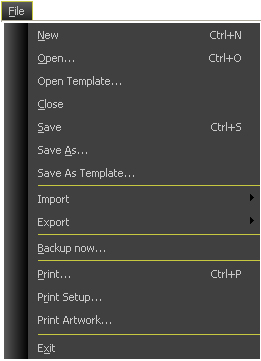
File menu
|
Top-level File menu
|
Import submenu
Export submenu
|
New command
The File > New command is one method of creating a new PCB design. It will invoke the Board Configuration Dialog to allow you to set board parameters or load a netlist unless you have checked the Do Not Show button in the Board Configuration dialog in which case a blank design is created.
Open… command
The File > Open command invokes a standard Windows file dialog that allows you to browse to and select one or more PCB123 design files. You can select multiple designs to open by holding down the Shift or Ctrl key while clicking on files. If you select multiple design files, each one will be opened in its own window.
Close command
The File > Close command closes the currently active design. If the design has been modified, you will first be prompted to save your changes.
Save command
The File > Save command writes a copy of the currently active design to disk using the same filename the design was opened with. If it is a new design that hasn’t been previously saved, then you will be prompted for a filename to save as (see below).
Save As… command
The File > Save As… command prompts you for a filename using the standard Window file dialog. This will write a copy of the currently active design to disk under the name supplied. If the file exists, you will be prompted to overwrite the existing file.
The entire state of your design is saved to disk with the exception of DRC markers and the local footprint cache. All display settings are saved in the file so the next time the file is opened it will appear the same as when it was saved.
Save As Template… command
The File > Save As Template… command saves the currently active design as a template for design reuse. Only a limited set of objects are saved as a template – specifically, board outlines, components, holes, text and board outlines. Net information and routing is not saved as a template, though this may change in the future.
You will be prompted for a descriptive name for the template and it will automatically be placed in the Templates subdirectory. The saved template is stored as a Sunstone NLF (Neutral Library Format) file. This is a fully encapsulated format. There are no external references. All data is represented in the file.
Import Gerber
PCB123 will allow you to import gerber and NC drill data. This is experimental and use it with caution. At this time the drill data does not import with the correct sizes and all negative polarity layers will not import correctly.
Import PCB123 XML
Import XML designs exported using PCB123’s export XML option. This provides you with an alternative method to view and edit your PCB123 design.
Export BOM command
The Export > BOM (Bill Of Materials) command outputs a BOM report for the currently active design. You will first be prompted for a report filename (default is design name with a .bom extension) and you will then be prompted to view the report.
The BOM report is a simple linear list of components alphabetically sorted by reference designator. In addition, each entry lists the components part type, footprint name, and the original component name if the component has been subsequently renamed.
Export Netlist command
The Export > Netlist command outputs a native PCB123 netlist report for the currently active design. You will first be prompted for a netlist filename (default is design name with a .net extension) and you will then be prompted to view the netlist.
There are two sections in the netlist report. The first section is a linear list of components alphabetically sorted by reference designator. The second section is a linear list of nets alphabetically sorted by net name. Inside each net there will be a list of zero or more component pins.
Export XML Data
Export your PCB123 design in XML format.
Backup Now… command
The File > Backup Now… command initiates an immediate backup of the currently active design.
Normally, in the course of design, PCB123 automatically saves a backup of all open designs once every ten minutes. It saves them to the Backup subdirectory using the name of the design and appending “_BACKUPn” where n is from 1 to 5, 1 being the most recent backup.
Print… command
The File > Print… command invokes the standard Windows print dialog and will print whatever is visible on the screen. It is meant for quick screen shots when you want a hard copy of some isolated section of the board or a reference print that is not scale dependent.
If you need scaled prints of the entire design use the Print Artwork command.
Print Setup… command
The File > Print Setup… command invokes the standard Windows dialog for configuring the print settings. Along with specifying the printer to use, this command can also be used to set paper sizes and orientation for print jobs.
Print Artwork… command
The File > Print Artwork… command invokes the Print Artwork dialog that allows you to do a detailed print that will match what you see on the boards that will be built. In fact, the Print Artwork command executes the same code that Sunstone generates Gerber files from with the exception of non-plated holes which are a special case to Print Artwork and will show up in the prints.
See the Print Artwork Dialog for more details.
Exit command
The File > Exit command exits the PCB123 program. You will be prompted to save any modified documents that you may have open.
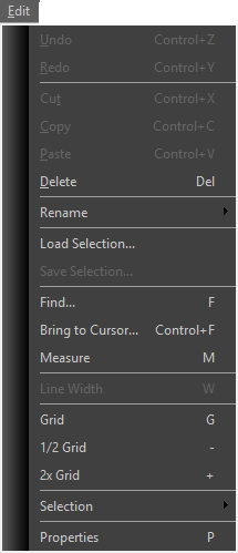
Edit menu
Top-level Edit Menu
|
Rename submenu
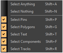
Selection submenu
|
Undo command
The Edit > Undo command undoes the last change to currently active design. Virtually all changes to the design are recorded and can be undone in the reverse order they were made. There is no limit to the size of the undo buffer other than memory limitations.
What constitutes a change for purposes of undo is operation dependent. In many cases an entire group of changes will be undone with a single undo command. For instance, selecting undo after an autoroute will undo the entire autoroute results, not just the last connection the autorouter completed.
When a change is undone, that change will be added to the Redo buffer in case you change your mind and want to redo it again. See below.
Redo command
The Edit > Redo command redoes the last undo operation. Repeated undo operations are stored to the redo buffer so you can redo a whole series of undo operations.
Cut command
The Edit > Cut command deletes the currently selected set of objects and places them into the paste buffer. There is only one paste buffer so only the last cut operation is available for paste.
See the Paste command for more information.
Copy command
The Edit > Copy command copies the currently selected set of objects into the paste buffer. There is only one paste buffer so only the last copy operation is available for paste.
See the Paste command below for more information.
Paste command
The Edit > Paste command makes a copy of the objects in the paste buffer and inserts them into the currently active design.
First, any components in the paste buffer are added to the design by assigning them a new reference designator that does not conflict with one already in the design. Their alpha-prefix is retained.
Next, any complete routes or connections that start and end at a pins that are also in the paste buffer will be added to the design. They will retail their original net name with a unique numerical suffix.
Lastly, all text and non-net-attributed board outlines will be copied without change. Net-attributed board outlines will either inherit a cloned net name or retain their original net names depending on whether their original net names were cloned during the paste operation.
After all objects are created, they will be in a selected state attached to the cursor ready to be placed.
Delete command
The Edit > Delete command deletes all selected objects from the currently active design.
The delete operation can later be undone.
Rename Net command
This command allows you to rename any existing net on the design.
Rename Part Command
This command provides a simple method to make corrections to part names without removing the part from the design. Change to the part name will show up in the bill of materials. Changing the part name does not update the library entry.
Rename Reference Designator
Change the reference designator for any single part.
Load Selection… command
The Edit > Load Selection… command is identical to the Paste operation except the pasted objects are from a previously saved set of objects or from a design template as opposed from the paste buffer. You will be prompted for a selection to load.
Currently this operation excludes any net information. A saved selection can contain everything except nets. See the Save Selection command for more information.
Save Selection… command
The Edit > Save Selection… command saves the selected objects from the currently active design to a disk file for later reuse. No net information is currently saved though this may change in the future.
This command is only available when you have an object or objects selected. Once invoked, you will be prompted for a description of the selection set.
Find… command
The Edit > Find… command prompts you for the name of an object in the currently active design and then centers the viewport on that object.
See the Find Dialog for more details.
Bring to Cursor… command
The Edit > Bring to Cursor… command is similar to the Find command but instead of zooming you to an object it selects the named object and snaps it to the cursor.
See the Find Dialog for more details.
Measure… command
The Edit > Measure… command activates the ruler and allows you to measure the distance between objects.
Line Width command
The Edit > Line Width command is only available when you are adding/editing polylines and routes. When selected, you will be prompted to enter a line width with the Line Width Dialog.
For polylines, the new line width applies to the whole polyline.
For routes, the new line width applies to the currently active line segment and subsequent segments you add to the route.
Grid command
The Edit > Grid command sets the working (snap) grid and the display grid for the currently active design. You can set the X and Y grid independent by separating the two values with a comma.
See the Grid Dialog for more details.
Select Pins command
The Edit > Select Pins command toggles the ability to select board-level pin objects in the currently active design or component pins in the Edit Footprint window.
Select Polygons command
The Edit > Select Polygon command toggles the ability to select Polygon objects in the currently active design.
Select Text command
The Edit > Select Text command toggles the ability to select text objects in the currently active design.
Select Components command
The Edit > Select Components command toggles the ability to select component objects in the currently active design.
Select Tracks command
The Edit > Select Tracks command toggles the ability to select track (route) objects in the currently active design.
Select Anything command
The Edit > Select Anything command turns on the ability to select all objects in the currently active design.
Select Nothing command
The Edit > Select Nothing command turns off the ability to select all objects in the currently active design.
Properties command
The Edit > Properties command is context sensitive. If you have nothing selected it invokes the Board Configuration Dialog. If you have one or more objects selected, then you will get a property page for each class of object selected.
See Object Property Pages for more information.
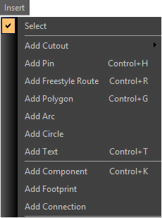
Insert menu
Top-Level Insert Menu
|
Add Cutout submenu
|
Select command
The Insert > Select command is the default state for selecting objects. When you stop adding or modifying objects by pressing the Escape key or selecting RMB-Cancel the system enters the Select state.
Add Cutout
The Insert > Add Cutout command allows you to choose to draw circular or rectangular cutouts. The cutouts are automatically added to the board outline layer. A cutout drawing using Draw Rectangle may have a maximum of four vertices.
Add Pin command
The Insert > Add Pin command immediately allows you to start adding pins to the currently active design or footprint.
When you first select this command, a pin will be attached to the cursor whose properties will be defaulted, usually to the same values as the last pin inserted.
By default, board-level pins do not have names, though they can be assigned names – even duplicate names. Board-level pins do not show up in a netlist report, only component pins do.
When creating a footprint, pins names start at 1 by default and increment from there. The only time a pin name can be reused in a footprint is if it has no name at all.
See the Pin Property Page for more information.
Add Freestyle Route command
The Insert > Add Freestyle Route command allows you to begin digitizing new route corners. You must start the new route from a pin or another route. If starting from another route, the new route will inherit the starting route’s layer and net.
If starting from a pin the new route layer will either be the pin layer in the case of a SMD pin or the current layer if it is a thru-hole pin. If the starting pin already has a net attribute then the route will inherit that pins net.
Once you have started routing you can digitize new corners by left-clicking the mouse and you can insert vias by changing layers or pressing the ‘Z’ key or change the current width by pressing the ‘W’ key.
To terminate a freestyle route you can press the escape key, click on another pin, or click on another track on the same layer as the last segment. If the new route has a temporary net then it will be ‘hardened’ by either inheriting the terminating objects net property or by creating a new net and assigning everything in the temporary net to the new net.
Add Polygon command
The Insert > Add Polygon command allows you to begin digitizing corners of polygon and polylines.
A polyline is a continuous series of line segments. They have a physical width and may be net attributed. In most cases polylines are not net attributed as they are widely used for nomenclature such as component outlines and title blocks.
A polygon is a closed 2-D surface. They do not have width. What you draw is the absolute edge of the polygon. They can be convex or concave but should not self-intersect.
If a board polygon has no net attribute, then the entire polygon is filled.
If a polygon does have a net attribute, then it becomes a copper pour and any object inside the polygon that does not have the same net attribute is “scratched” out of the polygon so as not to create a short. If a pin resides inside a copper pour polygon, and that pin has the same net attribute then the pin is cleared for thermal isolation but “spokes” are added between the pin and the copper pour to tie them together electrically. Determining where a thermal spoke is legal can be a fairly intensive calculation. Therefore what you see on the screen is only an approximation of the actual spokes. You must perform a Print Artwork to get a true representation of the thermal spokes.
See the Polygon Property Page for more information.
Add Arc command
The Insert > Add Arc command allows you to add arc objects to the currently active design or footprint by first defining one endpoint, then the other, and then adjusting the radius.
Arcs have definite width and are always chords of a perfect circle. They cannot be elliptical.
Add Circle command
The Insert > Add Circle command allows you to add hollow circle objects to the currently active design or footprint by first defining the circle center, and then sweeping out a radius.
Circles have definite width. They cannot be elliptical.
Add Text command
The Insert > Add Text command allows you to add rendered text “strings” to the currently active design or footprint. When you first select this command you will be prompted for the string to add with the Add Text Dialog.
Currently, only the ANSI character set is supported. Extended ASCII characters are not rendered but are stored in the string.
There is only one font available for text strings because the characters must be stroked and there is no reliable way to convert a TrueType font into a series of strokes that can be added to the board. This may change in the future.
Add Component command
The Insert > Add Component command allows you to interactively insert components into the active design.
When this command is selected the Add Component Dialog will be shown. After you select a part type or footprint with this dialog, a component will be created and snapped to the cursor ready for placement.
A unique reference designator (name) will be created for the component that uses the same alpha prefix as the last component added but with a unique numerical suffix.
These parts are footprints and symbols that have been paired and added to the PCB123 parts taxonomy.
Add Footprint command
Insert > Add Footprint allows you to select directly from the PCB123 footprint libraries and place parts on your layout. Once a footprint is placed on the layout, an auto created generic symbol is created and placed on the schematic sync page.
Add Connection command
The Insert > Add Connection command is really a tool that has a couple of features that allow you to define and modify nets.
The default mode for the tool allows you to specify point-to-point wiring for a net by first clicking on a component pin and then clicking on subsequent pins to define the connectivity of a net.
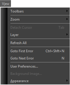
View menu
|
Top-level View menu
|
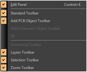
Toolbars submenu
|
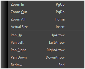
Zoom submenu
|
|
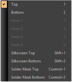
Layers submenu
|
Refresh All
The View > Refresh All command not only repaints the screen but refreshes the Object Hierarchy and rebuilds some internal tables. Pressing the Esc key when nothing is selected performs the same operation.
Goto First Error
The View > Goto First Error command zooms to, and centers the display around the first DRC error. If there are no DRC errors then you will be prompted to run a DRC.
Goto Next Error
The View > Goto Next Error command zooms to, and centers the display around the next DRC error. If there are no more DRC errors then you will be prompted to run another DRC and go to the first error found.
User Preferences…
The View > User Preferences… command is used to invoke the User Preferences Dialog.
Toolbars > Edit Panel
The View > Toolbars > Edit Panel command toggles the visibility of the Edit Panel.
Toolbars > Standard Toolbar
The View > Toolbars > Standard Toolbar command toggles the visibility of the Standard Toolbar.
Toolbars > Add Object Toolbar
The View > Toolbars > Add Object Toolbar command toggles the visibility of the Add Object Toolbar for either the layout or schematic.
Toolbars > Layers Toolbar
The View > Toolbars > Layers Toolbar command toggles the visibility of the Layers Toolbar.
Toolbars > Selection Toolbar
The View > Toolbars > Selection Toolbar command toggles the visibility of the Selection Toolbar.
Toolbars > Zoom Toolbar
The View > Toolbars > Zoom Toolbar command toggles the visibility of the Zoom Toolbar.
Zoom > Zoom In
The View > Zoom > Zoom In command increases the magnification of the display. If this command was invoked through the menu then the view center remains unchanged. If this command was invoked with the PgUp key then the view center will be where the cursor was when the command was invoked.
Zoom > Zoom Out
The View > Zoom > Zoom Out command decreases the magnification of the display. If this command was invoked through the menu then the view center remains unchanged. If this command was invoked with the PgDn key then the view center will be where the cursor was when the command was invoked.
Zoom > Zoom All
The View > Zoom > Zoom All command sets the screen magnification such that all objects fit on, and are centered on the screen.
Zoom > Pan Up
The View > Zoom > Pan Up command moves the view center up nearly one full screen height.
Zoom > Pan Left
The View > Zoom > Pan Left command moves the view center to the left nearly one full screen width.
Zoom > Pan Right
The View > Zoom > Pan Right command moves the view center to the right nearly one full screen width.
Zoom > Pan Down
The View > Zoom > Pan Down command moves the view center down nearly one full screen height.
Zoom > Redraw
The View > Zoom > Redraw command repaints the screen.
Layers > Top
The View > Layers > Top command sets the current layer to the Top layer. It also repaints the screen with the Top layer being painted last.
Layers > Bottom
The View > Layers > Bottom command sets the current layer to the Bottom layer. It also repaints the screen with the Bottom layer being painted last.
Layers > Inner1
The View > Layers > Inner1 command sets the current layer to the Inner1 layer. It also repaints the screen with the Inner1 layer being painted last. This command will only be available if the current design has more than 2 layers.
Layers > Inner2
The View > Layers > Inner2 command sets the current layer to the Inner2 layer. It also repaints the screen with the Inner2 layer being painted last. This command will only be available if the current design has more than 2 layers.
Layers > Inner3
The View > Layers > Inner3 command sets the current layer to the Inner3 layer. It also repaints the screen with the Inner3 layer being painted last. This command will only be available if the current design has more than 4 layers.
Layers > Inner4
The View > Layers > Inner4 command sets the current layer to the Inner4 layer. It also repaints the screen with the Inner4 layer being painted last. This command will only be available if the current design has more than 4 layers.
Layers > Silkscreen Top
The View > Layers > Silkscreen Top command sets the current layer to the Top Silkscreen layer. It also repaints the screen with the Top Silkscreen layer being painted last.
Layers > Silkscreen Bottom
The View > Layers > Silkscreen Bottom command sets the current layer to the Bottom Silkscreen layer. It also repaints the screen with the Bottom Silkscreen layer being painted last.
Layers > Soldermask Top
The View > Layers > Soldermask Top command sets the current layer to the Top Soldermask layer. It also repaints the screen with the Top Soldermask layer being painted last.
Layers > Soldermask Bottom
The View > Layers > Soldermask Bottom command sets the current layer to the Bottom Soldermask layer. It also repaints the screen with the Bottom Soldermask layer being painted last.
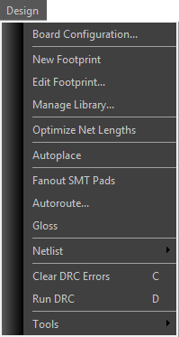
Design menu
|
Top-level Design menu
|
Netlist submenu
Tools submenu
|
Board Configuration
The Design > Board Configuration command invokes the Board Configuration Dialog which is where you set such parameters as the number of layers, whether or not you want soldermask, etc.
New Footprint
The Design > New Footprint command creates a new, unnamed, empty footprint and switches the view to the Footprint Editor.
Edit Footprint
The Design > Edit Footprint command invokes the Library Browser (same as the load part dialog) so you can select a footprint to edit. Once you have selected a footprint then that footprint will be loaded into a Footprint Editor for you to modify and save.
Manage Library
The Design > Manage Library command invokes the Library Manager Dialog which lets you perform such operations as create new libraries, catalog existing libraries, and cut and paste among libraries.
Optimize Net Lengths
The Design > Optimize Net Lengths command works only on unrouted portions of nets, not existing routing. The left side of the picture below contains a net before optimization and the right side after optimization. You can override this behavior on a per-net basis by setting the Do Not Optimize flag in the Net Properties dialog.

Autoplace
Design > Autoplace makes a best effort attempt to place components on the layout board in a manner that minimizes overall routing complexity. The Autoplace function is not designed to be exhaustively accurate, but rather as a convenience to get you started as you complete schematic design and transition to the early stages of physical layout.
Fanout SMT Pads
The Design > Fanout SMT Pads command automatically routes out any connection tied to a SMT (surface mount) pad and then terminates at a via as pictured below.

If a connection coming out of a surface mount pin needs to be tied to a plane then fanning it out basically completes the connection to that pin and the ratline will disappear. Fanout also aids a very important routing strategy for high-density SMT boards. Because the surface layers on these boards are highly congested with pads most of the routing has to take place on inner layers. A smart strategy to get to these inner layers is to fanout the board early in the design process – preferably before any other routing.
Autoroute
The Design > Autoroute command attempts to automatically complete all routing on the board. A reasonable set of defaults are used by the router but a detailed explanation of possible settings that can control the router can be found under Autorouter User Preferences.
Gloss

The Design > Gloss command automatically performs aesthetic rerouting. It typically removes redundant corners and segments, often spreads routes out, and generally fixes such minor problems as acute angles and 90-degree bends. An example is shown below.
Netlist
Access the netlist management forms.
Compare/Update Design
The Design > Netlist > Compare/Update Design command loads a master netlist from disk, converts it to a PCB, and detects any differences between the master PCB and the current slave PCB. The difference list is then optimized to a set of changes that will have the least impact in the board. The list will then be presented to you in the form of an ECO Report Dialog. When this dialog is dismissed you will then have the option of automatically performing the changes that will make the slave match the master.
Even if there were no changes detected during the comparison all component footprints will be updated from the master.
Manage Stored Part Associations
This form allows you to update any previously defined parts associations for use in future projects where a netlist will be imported into PCB123.
Clear DRC Errors
The Design > Clear DRC Errors command will simply delete all the DRC markers from the current design. DRC markers are generated from running the DRC command or interactively while editing your design.
Run DRC
The Design > Run DRC (Design Rule Check) command performs the following checks on all objects in the current design:
Track-To-Track Spacing Violation – Two tracks (routes) from different nets are less than the required minimum distance apart.
Track-To-Pad Spacing Violation - A track and a pad from different nets are less than the required minimum distance apart.
Track-To-Via Spacing Violation - A track and a via from different nets are less than the required minimum distance apart.
Track-To-Board outline Spacing Violation - A track and a board outline from different nets (or board outline with no net) are less than the required minimum distance apart.
Track-To-Text Spacing Violation - A track and a piece of text are less than the required minimum distance apart. This will result in overlapping or unreadable text.
Pad-To-Pad Spacing Violation – Two pads from different nets are less than the required minimum distance apart.
Pad-To-Via Spacing Violation – A pad and a via from different nets are less than the required minimum distance apart.
Pad-To-Board outline Spacing Violation – A pad and board outline from different nets (or board outline with no net) are less than the required minimum distance apart.
Pad-To-Text Spacing Violation – A pad and a piece of text are less than the required minimum distance apart. This will result in overlapping or unreadable text.
Via-To-Via Spacing Violation – Two vias from different nets are less than the required minimum distance apart.
Via-To-Board outline Spacing Violation – A via and a board outline from different nets (or board outline with no net) are less than the required minimum distance apart.
Via-To-Text Spacing Violation – A via and a piece of text are less than the required minimum distance apart. This will result in overlapping or unreadable text.
Board outline-To-Board outline Spacing Violation – Two board outlines from different nets are less than the required minimum distance apart.
Board outline-To-Text Spacing Violation – A board outline and a piece of text are less than the required minimum distance apart. This will result in overlapping or unreadable text.
Text-To-Text Spacing Violation – Two pieces of text are less than the required minimum distance apart. This will result in overlapping or unreadable text.
Object-To-Board Outline Spacing Violation – A route, pad, via, board outline, or piece of text is too close to the board outline.
Drill-To-Drill Spacing Violation – Two holes overlap at offset locations. This condition will result in a broken drill bit.
Unfinished-Route Violation – There is a connection between two pins that still needs to be routed to complete the circuit.
Board-Too-Small Violation – The minimum dimension in either the x or y axis is ¼ inch. If you receive the Board-Too-Small violation, then the board is less than ¼ inch in either axis. We cannot manufacture a board that small.
Silkscreen-Over-Pad Warning – Silkscreen outline or text runs into a pad that is unmasked. This is a problem for the fabrication process as well as possibly making the silkscreen illegible.
Dangling-Trace Warning – A route does not end at a pad, via, or other route. Traces in this configuration creates an antenna effect. While the antenna may be intentional, PCB123’s DRCs will alert you to the condition as a precaution.
Pad-Annular Warning – The pad size minus the drill size is less than the recommended minimum.
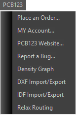
PCB123 menu
MY Account…
The PCB123 > My Account… command will invoke a browser session to your account status page at Sunstone.com. Once you’ve logged in, you can view your personal account settings including: your default user preferences (shipping address, carrier, payment method, etc.); personal profile information (name, company, email, etc.); and recent order activity including current status for any orders in process.
PCB123 Website…
The PCB123 > PCB123 Website… command will invoke a browser session at www.sunstone.com
Report a Bug…
The PCB123 > Report a Bug… command will invoke a browser session and take you to the Contact Us page for technical support on the www.sunstone.com website. From here you can report the bug details. Customer Service will acknowledge receipt of your bug report, and follow up with you as necessary.
Density Graph
PCB123 sample plug-in.
DXF Import/Export
This is a sample PCB123 plug-in to import/export a simple DXF board outline and mounting holes. This plug-in does not support arcs in the board outline. Only the board outline and holes that are not part of footprints or connected to traces will be exported.
IDF Import/Export
Similar to DXF plug-in. This sample plug-in allows you to import/export the board outline and mounting holes in IDF format.
Relax Routing
PCB123 sample plug-in.
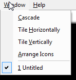
Window menu
Cascade
The Window > Cascade command will rearrange open design windows into a cascading pattern.
Tile Horizontally
The Window > Tile Horizontally command will rearrange open design windows into a horizontal tiled pattern.
Tile Vertically
The Window > Tile Vertically command will rearrange open design windows into a vertical tiled pattern.
Arrange Icons
The Window > Arrange Icons command will move any iconized design files into an orderly row across the bottom of the PCB123 editing pane background.
Toolbars
Add Object toolbar

The Toolbars > Add Object Toolbar command toggles the visibility of the Add Object Toolbar. The Add Object Toolbar gives quick and easy access to commands for adding objects to the schematic, including” Title Bar info; component symbols; polylines; board outlines; arcs; circles and text.
Layer toolbar

The Toolbars > Layer Toolbar command toggles the visibility of the Layers toolbar. The Layers toolbar typically displays vertically, along the right edge of the PCB123 application window. The Layers toolbar provides one-click view filtering for all layers specified in the currently active edit panel.
Selection toolbar

The Toolbars > Selection Toolbar command toggles the visibility of the Selection toolbar. The Selection toolbar typically displays vertically, along the right edge of the PCB123 application window. The Selection toolbar provides one-click view filtering for selectable items in the layout editing panel.
Zoom toolbar

The Toolbars > Zoom Toolbar command toggles the visibility of the Zoom toolbar. The Zoom toolbar typically displays vertically, along the right edge of the PCB123 application window. The Zoom toolbar provides one-click view adjustment in the edit window
3-D View toolbar
Wireframe
The 3D > Wireframe command disables the 3D view’s solid surface rendering feature. This view often allows for close viewing of vias and traces in multi-layer designs. Wireframe can also provide a faster rendering of the 3D model on some computers.
Show Silkscreen
By default, the 3D view displays the silkscreen layer data. Turning the 3D – Show Silkscreen command off removes silkscreen data from the 3D model.
Panels
Display panel
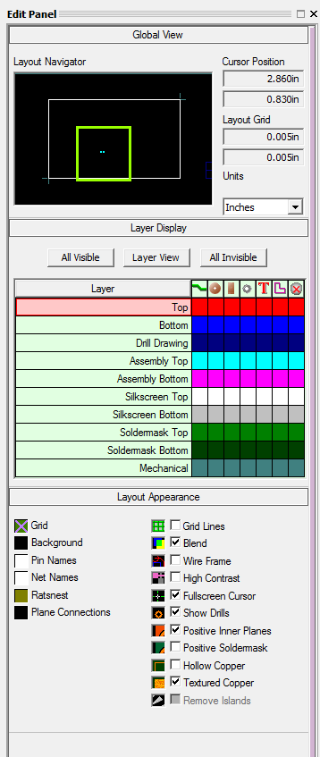
The Display Panel provides easy access to layout window display parameters to assist in the design creation, review and editing process. The display panel contains three major functional regions: the Global View, the Appearance menu, and the Layer Display.
Global View provides the user with a thumbnail view of the entire design space. A ghost rectangle shows the current zoom and pan location for the edit window. As the edit view zooms in further, the ghost rectangle naturally gets smaller. By dragging/dropping a rectangle directly on top of the Global View, you can quickly reset your edit pane view to a new location without tedious panning and zooming commands.
Also in the global view are a read-only display of the current cursor position coordinates, a read-only view of the current grid space settings, and user-selectable units for reporting positions in the design space. The available units include: Inches; Mils, Centimeters and Millimeters.
The Appearance region allows you to change the rendering for grids, backgrounds, ratsnest data, layer data blending and other methods for customizing the representation of your design. These tools allow you some sophisticated methods for managing the context data represented around your current area of concentration. Many of these appearance features can also be edited on the User Preferences dialog. A functional description for each attribute on the appearance page can be found in the User Preferences Display Page section.
The Layer Display region allows the user to turn layers and data types on or off. Presented in tabular view with rows representing a layer and columns representing a data type, users can interactively select the data to display. This technique comes in handy when concentrating on data for a specific layer, such as a ground plane or component/connector escape routing.
Parts panel
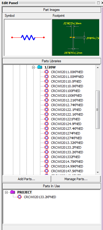
The parts panel allows you to search for parts that are listed in the PCB123 parts libraries. These are parts that have footprints that are paired with schematic symbols. These parts often have additional properties associated with them to further specify the parts type and characteristics. Many of the parts listed in the Ultra Library contain Digi-key part numbers.
Once you select a part from the library you are provided with a preview of both the symbol and footprint to aid in parts selection. The Add parts button found in this panel provides an alternative window to search through the libraries. The Add Parts window allows you to see lists of parts that match your search criteria.
Using the Manage Parts button you can add or remove parts from the Parts Libraries. Here you can match previously created footprints and symbols to create new parts to use in your layouts and schematics. The Parts In Use section of this panel provides a list of all of the parts that have ever been added to your design. You can select parts from this area and place them on your layouts and schematics.
Project panel
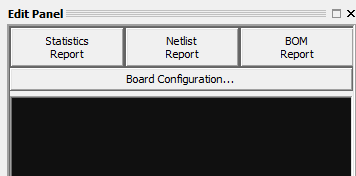
Unlike the Display Panel, the Project Panel stays the same for all tabbed views of the design. The Project Panel displays three buttons across the top: Statistics Report; Netlist Report; BOM Report. Each of these three buttons generates an ascii format report based on your current design.
The Board Configuration area provides an interactive tree-style hierarchical access to all the design primitives: nets, components, pins, etc. and the associated meta-data. Properties can be edited from this location so care must be used by casual users not to inadvertently change their design.
The Schematic Properties provide an interactive area for setting and adjusting line styles, text fonts and styles, and data fields for the design title block.
DRC/ERC panel
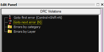
The DRC/ERC panel contains a live listing of all the current design violations in the project.
The DRC will report on shorts, opens, and violations of manufacturing rules such as minimum spacing between objects of different nets, and pad size vs. drill size violations.
Locations of errors reported by the DRC are marked with a grey circle-? icon. By hovering the mouse pointer over the error, users can access a summary explanation for the cause of the error being reported.
The DRC/ERC tab also allows users to access violations by category or by layer. At the top of the DRC/ERC tab are the ‘stepper’ functions, allowing users to move from error to error so as to view/fix each one interactively.
Context Panes
Pin properties
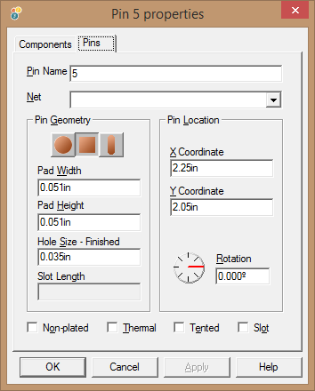
On the Pins tab, a selected pin will present its information here. The Pin Name and optionally-assigned Net name are editable. The Pin Geometry parameters allow for specification of the pin shape, height and width, and the hole size (for thru hole parts). The Pin Location section allows users to reposition or rotate the pin to achieve customize or correct parts.
By selecting individual pins, users can achieve pin-by-pin access to the pin properties on the selected component.
Please note that unless the part is a user-specified custom part, it is not recommended practice to change the pin geometry or location information.
Component properties
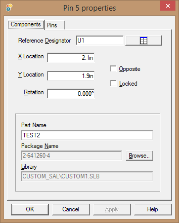
On the components tab, shown here, users can change the Reference Designator, x location, y location and component rotation. Changing the values for these three parameters will move the component origin to the newly specified settings. Please note that this may cause the component to move away from any previously placed traces.
The Opposite checkbox will move the component to the opposite side of the board. When checked, the component will be on the BOTTOM layer; when unchecked, the component is on the TOP layer.
Part Type and Packaging can also be specified from the Component Properties pane.
Object properties
 |
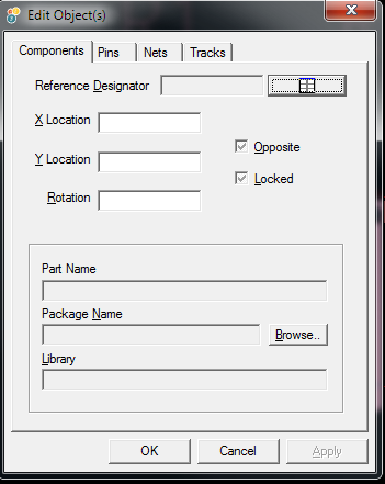 |
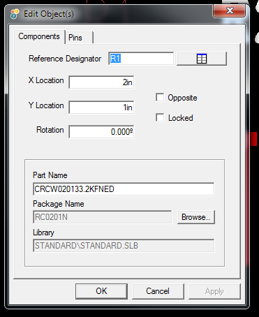
This page changes depending upon what is selected.
Polygon properties (Schematic)
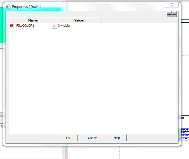
The Polygon properties view offers two ways to interact with polygon properties. Selecting the Properties menu pick from the right-click menu presents the following properties table. Users can add, delete and specify properties as needed to change the character of the polygon.
When the polygon is selected, the Edit Panel also allows access to some commonly used polygon properties.

Here the user has access to Line Width, Line Style, and Fill Style. The user Also can specify an Identifier, choose the line color, and fill color.
Text properties (Schematic)

The Text properties view is available from the right mouse menu on a selected text instance. Text properties presents the user with a tabular dialog in which the user can add properties and specify values for the text box selected. By default, the Text properties dialog uses the text defaults, and no specific overriding properties are on the list. In this example, the user has specified properties that will affect only the selected text.
Dialog Boxes
About… Dialog
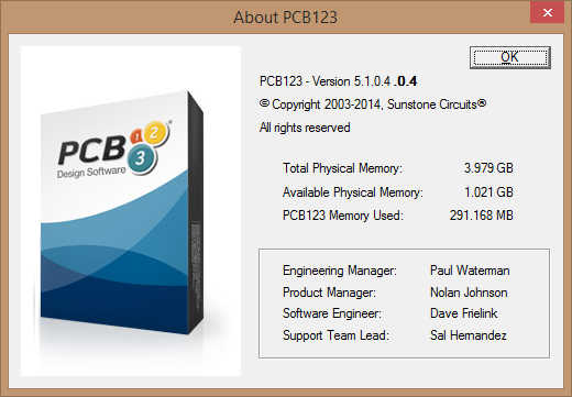
Besides some shameless vanity information, the Help > About… dialog tells what version of PCB123 you are running and how much memory the software is using.
Add Text Dialog
The Add Text Dialog is invoked when the Text Tool  is selected in current design or footprint. It simply prompts you for the string of text to add.

Board Configuration Dialog
The Board Configuration Dialog is invoked from the Design menu or by RMB Properties when nothing is selected. It will also be shown when you choose to bypass the New Board Wizard and select File/New in which case additional fields will be activated that allow you to load a netlist for instance.
It is primarily used to specify various board manufacturing parameters.

The Board Name field is simply a label for your design. There are no restrictions on it.
The Board Size X and Y fields specify the rectangular size of the board. These fields are only active when this dialog is invoked in response to File/New, otherwise they are grayed out and only inform you of the existing current board size.
The Netlist File Name field can only be used when this dialog is invoked from File/New. It is used to specify a netlist or netlists to load into the new design.
The Layers Required field is where you can specify the number of layers in your design. The default is two layers but if you choose more than two then other options will be enabled such as plane layer assignments. If you invoked this dialog from Design/Board Configuration on an existing design and you decrease the layer count then objects on the deleted layers will be permanently removed from the database. Any routing on the removed layers will be unrouted and the ratsnest possibly updated.
The Power Planes checkboxes are only enabled when you specify more than two layers for your design. When they are enabled you can check which layers will be treated as poser planes. Nets that get assigned to power plane layers are assumed to be connected as soon as something in the net touches a plated-through-hole.
The Solder Mask checkbox is only enabled for two and four layer boards. Six layer boards automatically get a solder mask. Solder mask, also known as solder resist is a green coating that is uniformly applied to the board except where solderable surfaces are required such as pads. You must check Solder Mask if you want silk screen on your board. There is an additional manufacturing charge for selecting solder mask.
The Silk Screen radio buttons are only enabled if you have solder mask enabled. You can choose to have no silk screen, silk screen only on the top layer, silk screen only on the bottom layer, or silk screen on both top and bottom. If you choose to have silk screen on the bottom layer (or both top and bottom) then there is additional fixed cost applied.
The Material Thickness is almost always 0.062”. There are several restrictions placed on a 0.031” board which are the board can only be a two-layer board, must have solder mask, and cannot have a 2.5oz copper weight.
The Finished Copper Weight option is almost always 1oz. There are several restrictions placed on a 2.5oz copper board which are the board can only be a two-layer board, must have solder mask, and cannot be 0.031” thick.
The Quantity drop list is where you specify how many boards you want to build. You can select between 2 and 100 boards indifferent increments. The price-per-board and the lead time is impacted by the quantity. You can freely experiment with this setting.
The Check If You Do Not Want This Displayed button can prevent this dialog from being displayed when you use File/New. This can always be unchecked by invoking this dialog in Design/Board Configuration.
Change Grid Dialog
The Change Grid Dialog is nearly universal in the system and can be invoked while doing other tasks such as moving a component. The simplest way to invoke the Change Grid Dialog is to press the G key on your keyboard but you can also choose Edit > Grid from the menu bar.
The New Grid field is where you specify the desired grid. You can specify independent X and Y axis grids by separating the two with a comma. Specifying only one value implies that both the X and Y grid will be the same.
Component Property Page
The Component Property Page is invoked whenever a component is selected and Properties is chosen either by pressing Alt+Enter on your keyboard or RMB/Properties. It can also be invoked by selecting a component in the Object Hierarchy tree and selecting RMB/Properties.

If you only have components in your selection set then the only tabs that will appear in the property pages are components and pins. Otherwise other object tabs may be present too.
If you only have one component selected then all the fields in the Component Property Page will be filled in with the values from that component. If you have more than one component selected then the fields will be empty or in an indeterminate state. Any field left empty or indeterminate when the page is dismissed will be unchanged in the selected components.
The Reference Designator field (or component name) is the name to assign to the component. It will be forced to upper case and it must be unique in the design. If more than one component is selected then this field will be disabled. Any change to the reference designator here will also be reflected in the companion schematic.
The Component Attributes button  can be pressed to invoke the Attributes Dialog.
The X Location field is where the component is located in the X-axis of the design. It will default to the current units but can be in the format of your choice. The X location is relative to the component’s local origin.
The Y Location field is where the component is located in the Y-axis of the design. It will default to the current units but can be in the format of your choice. The Y location is relative to the component’s local origin.
The Rotation field is the component rotation about its local origin. Rotations are counter-clockwise unless you enter a negative number in which case they are clockwise but will be converted to the appropriate positive rotation when this dialog is dismissed.
The Opposite button, when checked, signifies that the component is on the back side of the board. A component on the back side is automatically mirrored.
The Part Name field may or may not be filled out depending on how the component was originally loading into the design. If the component was referenced from a Library part as opposed to a Footprint then the Part Name field will be the name of the device. This field can be used to substitute a part for another in the Pats Libraries. Type in the name of another part from the Parts libraries and press Tab and PCB123 will update the footprint, schematic and bom with the new part.
The Package Name field contains the name of the footprint this component uses and is not directly editable but can be filled in by the Part Browser dialog. If you select a different footprint for this component the new footprint must contain pins that will match up with the current nets used by this component. I.E. it cannot change the netlist.
Create New Library Dialog
The Create New Library dialog can be invoked either from the Library Manager or when saving a footprint in the Footprint Editor.
Why would you want to create a new library? Library management is a highly subjective topic leading to many lively debates but here are some facts:
You don’t want to save custom footprints into any standard library that is supplied with the software because they may possibly be overwritten the next time you update to a newer revision.

There is no penalty in creating new libraries. Part searching by default spans all libraries in and under the Lib directory.
By placing custom footprints for a particular design into its own library, you most likely will not have any naming conflicts with other parts of the same name but different content. The library will also have a small size that is easily copied from machine to machine.
The Library Name field is where you define the name of the library you are creating. It will automatically be put into the Lib/Custom directory.
The Description field is where you can enter a brief description of the library you are creating.
ECO Report Dialog
The ECO report dialog is automatically displayed when you perform a Design/Compare Netlist and there are differences between the netlist and the design.

The Print button  can be used to generate a hardcopy of the change report.
Find Object Dialog
The Find Object dialog is invoked by pressing the ‘F’ key on your keyboard or by selecting Edit/Find from the menu bar. It is used to locate a named object and center it on the screen. This same dialog will be invoked by the Snap Object to Cursor command which instead of zooming to the object will actually move the object to the cursor.

The Name of Item to Find field is where you specify the named item or sub-item to find. Sub-items are specified by separating the item and sub-item name with a period. For instance:
U1 will center the screen on the origin of component U1.
U1.3 will center the screen on pin ‘3’ of item U1.
Key Assignments Dialog
The Key Assignments Dialog can be invoked under Help/Key Assignments. By pointing at a key on the pictorial keyboard or actually typing a key on your physical keyboard you will be presented with information on what that key does by itself or when the Ctrl or Shift key is held in combination.

Line Width Dialog
The Line Width dialog can be invoked from the File/Edit menu, from various context menus, or by pressing the ‘W’ key. It is used to change the width of any line object being drawn. If you invoke this dialog while routing, then the new width will apply to the segment from the last corner clicked and all subsequent corners until you stop drawing or change the width again.

The Line Width field is where you specify the new width. It will default to the current units but can be in the format of your choice.
Load Part Dialog (simple mode)

The Load Part dialog is invoked in many ways. It may be invoked while loading a netlist when a part type cannot be found in the library. It will be invoked when you choose to add a part manually using the Add Footprint Tool or edit the footprint properties of an existing component.
The Search drop list is where you enter the part search criteria. The drop list contains the last five searches performed. The search criteria may contain the wildcards ‘*’ and ‘?’. The ‘*’ wildcard means match anything after the criteria and the ‘?’ means match any character in that position. Example: searching for DIP* will match DIP8, DIP14, etc. Searching for DIP?0 will match DIP10, DIP20, etc. By default all libraries are scanned for a Part Type, Footprint, or a description field that matches the search criteria.
The Begins With and Contains radio buttons are used to expand or limit the scope of the search criteria. When you have the Begins With radio button checked, only items whose name begins with the search criteria are matched.
The Go button will initiate a search of the libraries. Any item matching the search criteria will be listed in the Select list and the first item highlighted and displayed in the Preview Pane.
The Advanced Search button expands the dialog to include additional options found in the Advanced Mode of this dialog.
The Select list contains all the items that match the search criteria. The name, the number of pins in the part, and the computed X and Y pitch (spacing between pins) will be displayed for each matching item. The computed pitch will be shown in inches if the pitch happens to divide evenly into .005” otherwise it will be shown in millimeters.
The Preview pane shows a graphical view of the currently selected item.
The text of the Insert Selection button may change based on the context of how this dialog was invoked but its action is to dismiss the dialog using the currently selected item.
Load Part Dialog (advanced mode)
The Advanced Mode of the Load Part dialog is the same as the Simple Mode except for the following additional items described below:

The Library Tree shows the hierarchical structure of the Lib directory and all subdirectories. You may check and uncheck individual libraries or folders to include or exclude them from the search. You may also click on an individual library to list the entire contents of that library in the Select list.
The Footprints Used list will be filled in if you have selected a Part Type in the Select list as opposed to a Footprint. Some libraries contain Part Types such as 74LS00 and those Part Types may list multiple footprints that can be used.
The Footprint Details section lists various properties of the currently selected footprint.
Load Selection Dialog
The Load Selection Dialog can be invoked either by choosing Edit/Load Selection from the menu bar or by RBM with nothing selected and choosing Load Selection from the context menu.
This dialog will allow you to merge an existing template or a previously saved selection into your design.

The Item list contains all the named templates/selections you have. When you click on one it will be previewed in the Preview Pane. The previewed item will be merged into your design when select Ok.
Manage Library Dialog
The Manage Library dialog packs a big punch in a small area. It can be used to create and delete libraries, copy, move, and delete library contents, and even create a web-based visual catalog of library contents.

The dialog is broken into four areas with simplest being the Preview pane that simply displays the selected part type or footprint. The other three sections each contain a list and a toolbar to perform various operations on the lists.
The Libraries list contains all the individual library files in the Lib directory and subdirectories. If you have not selected any libraries then the only toolbar option available will be the Create New Library button  . You may select multiple libraries by holding down the Shift or Ctrl keys while clicking on library items. When one or more libraries are selected all the library tools will be available. They are as follows:
 Import NLF Items into selected libraries. This command will prompt you for the name of a PCB123 Neutral Library Format file that may contain part types and footprints to add to the selected libraries.
 Create a new library. This command will create a new library in the Custom subdirectory using the Create New Library Dialog.
 Delete selected libraries. This command will delete the selected libraries from your disk. Use with caution.
 List contents of selected libraries. This command will generate a columnar list of all items in the selected libraries as shown below.

 Generate HTML catalog of selected libraries. This command generates an HTML table with statistics and images of all the items in the selected libraries as shown below.

The Part Types list contains all of the part types found in all the selected libraries. The Part Type Tools will be disabled until you select one or more part types. You may select multiple part types by holding down the Shift or Ctrl keys while clicking on part type items. The Part Type Tools are as follows:
 Delete Selected Part Types. This command removes the selected part types from their respected libraries. This is not an undoable operation and you will be prompted for confirmation.
 Cut Selected Part Types. This command removes the selected part types from their respected libraries and places them in the paste buffer. You can then select a different set of libraries and paste the part types into them, effectively moving them from one library to another.
The Footprints list contains all of the footprints found in all the selected libraries. The Footprint Tools will be disabled until you select one or more footprints from the list. You may select multiple footprints by holding down the Shift or Ctrl keys while clicking on footprint items. The Footprint Tools are as follows:
 Delete Selected Footprints. This command removes the selected footprints from their respected libraries. This is not an undoable operation and you will be prompted for confirmation.
 Cut Selected Footprints. This command removes the selected footprints from their respected libraries and places them in the paste buffer. You can then select a different set of libraries and paste the footprints into them, effectively moving them from one library to another.
Merge Nets Dialog
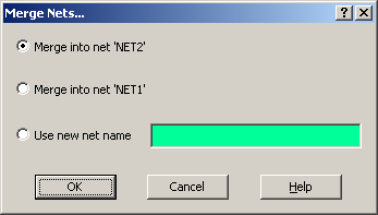
The Merge Nets Dialog is only invoked when you are in the Connection Tool and you attempt to add a connection between two different nets. Because the two nets must become one, this dialog is provided as a convenience to resolve the final net name.
The two Merge into ‘Netxxx’ radio buttons let you choose to use one of the existing nets. ‘Netxxx’ is actually a placeholder. The real net names will appear in its place.
The Use New Net Name radio button, when checked, will allow you to enter a completely different net name for the resulting net. The net name you enter must not already exist in the design.
Net Property Page

The Net Property Page is invoked whenever a net or track/connection is selected and Properties is chosen either by pressing Alt+Enter on your keyboard or RMB/Properties. It can also be invoked by selecting a net in the Object Hierarchy tree and selecting RMB/Properties.
If you only have nets or tracks/connections in your selection set then the only tabs that will appear in the property pages are Nets and Tracks. Otherwise other object tabs may be present too.
If you only have one net selected then all the fields in the Net Property Page will be filled in with the values from that net. If you have more than one net selected then the fields will be empty or in an indeterminate state. Any field left empty or indeterminate when the page is dismissed will be unchanged in the selected nets.
The Net Name field is the name to assign to the net. It will be forced to upper case and it must be unique in the design. If more than one net is selected then this field will be disabled.
The Width field is the default width for tracks in this net. You cannot change existing track widths by changing this field. You must use the Track Property Page for that. The width will be clamped to a range whose maximum must not exceed ½ inch. The minimum width will typically be .007” unless the board is configured to use 2.5oz copper in which case the minimum width will be .012”.
The Spacing field is where you can enter the minimum required spacing for this net or nets. It is typically .007” unless the board is configured to use 2.5oz copper in which case the minimum spacing will be .012”. Any physical object that does not belong to this net must meet or exceed this spacing or a DRC error will be issued.
The Via Size field is where you specify the default via size for any vias belonging to this net. It is typically defaulted to the smallest size allowed for the given board configuration. You should only change this for special circumstances such as you feel that a via in this net may carry a large current.
The Drill Size field is where you specify the default via drill size for any vias belonging to this net. It is typically defaulted to the smallest size allowed for the given board configuration. You should only change this for special circumstances such as you feel that a via in this net may carry a large current.
The Net Color button can be used to select the color of the ratsnest for the selected net or nets. This does not affect the color of routes, only the unrouted connections. This can be useful during the placement of components. Critical nets can be set to a different color for easy identification of the net’s topology.
The Routing Priority slider is only used by the autorouter. You typically do not need to set this except for unusual circumstances where you feel this net might need the most direct routing and therefore should be routed early in the process. To set the priority low really means that everything else is a high priority except this net.
The Assigned to Plane Layers checklist will only be available if you have set up plane layers in the Board Configuration. If you have, you can signify that this net is to be assigned to one or more of the plane layers. When a net is assigned to a plane layer then any drill in the net will constitute a plane “hit” and will be tied to that plane layer through a thermal relief.
The Do Not Optimize checkbox, when checked, will honor the current connection topology or connection ordering. The default is off which results in a dynamic shortest-length connection ordering based on the relative locations of all the pins in the net.
Package Print Dialog
The Package Print Dialog in invoked when you are in the Footprint Editor and choose Print from the File Menu. It is used to print a hardcopy of the currently active footprint.

The X-Shift and Y-Shift fields are used to specify an offset for the footprint. The page origin is the lower-left of the page so positive X shifts are to the right and positive Y shifts are up.
The Rotation drop list allows you to choose an orthogonal rotation for the footprint when it is printed.
The Scale field is used to specify a scale factor for the footprint when it is printed. It is a scalar value and not a ratio. 2.0 is double scale, 0.5 is half scale.
The Mirror checkbox, when checked, will flip the footprint image as though you were looking at it from the back.
Pin Property Page

The Pin Property Page is invoked whenever a component or pin is selected and Properties is chosen either by pressing Alt+Enter on your keyboard or RMB/Properties. It can also be invoked by selecting a component or pin in the Object Hierarchy tree and selecting RMB/Properties.
If you only have components and pins in your selection set then the only tabs that will appear in the property pages are components and pins. Otherwise other object tabs may be present too.
If you only have one pin selected or one single-pin component then all the fields in the Pin Property Page will be filled in with the values from that pin. If you have more than one pin selected then the fields will be empty or in an indeterminate state. Any field left empty or indeterminate when the page is dismissed will be unchanged in the selected pins.
The Pin Property Page is the only mechanism for drilling down into a component without editing that component in the Footprint Editor.
The Pin Name field is where you label this pin. If you have multiple pins selected this field will be disabled. Pins can be unlabelled and net connected but they will not appear in any netlists or reports. Pins that belong to components must be unique unless unnamed. Pin names will be forced to use upper case.
The Net Name drop list is where you can assign or reassign a net to this pin. If this property page was invoked from the Footprint Editor then this field will be disabled.
The Round Pad Shape button  sets the shape of this pin to round. Only the pad width needs to be filled in.
The Rectangular Pad Shape button  sets the shape of this pin to a square or rectangle. Both the pad width and height need to be filled in.
The Oblong Pad Shape button  sets the shape of this pin to a rectangle with rounded ends. Both the pad width and height need to be filled in and if they are the same value then the result will effectively be a circle.
The Pad Width field is used to specify the width of rectangular and oblong pads and the diameter of round pads.
The Pad Height field is only enabled for rectangular and oblong pads. It specifies their height. It must not be zero.
The Hole Size is used to specify the finished (final) hole size for a pin. Zero is valid, indicating a surface mounted pin. The available hole sizes changes between plated and non-plated holes. The Pad Size must be larger than the hole size plus a minimum annular ring that will change depending on the copper height of the board and the diameter of the hole. The typical minimum annular ring is 0.008”.
The Slot Length sets the length of a slot. Plated slots must have a pad annular ring and the guidelines are the same as those set for holes.
The Non-Plated checkbox, when checked, signifies that the hole will not be plated and therefore not conduct electricity. They are typically used for mounting and tooling holes.
The Thermal check box determines how a through-hole pin or surface mount pad will connect to a plane or filled polygon. Checking the pin will connect with a thermal relief. Un-checked the pin will connect directly to a filled polygon with copper flooding all the way to the pads edges.
The Tented check box determines if a pin or surface mount pad is covered by solder mask or not. With the box checked a pin/pad will be covered by mask. Un-checked the pin/pad will have a solder mask opening.
The Slot check box activates the slot length field and allows you to create slots in your pcb designs.
The Pin Location X and Y fields are used to position the pin. The coordinate system used depends on the ownership of the pin. If the pin belongs to a component then the location will be relative to the component’s origin. If the pin is a free-standing board-level pin then the location will be relative to the board origin.
The Pin Rotation field and spin control are used to specify the pin rotation in the pin’s own local coordinate system. Pin rotations are counter-clockwise unless you enter a negative number in which case they are clockwise but will be converted to the appropriate positive rotation when this dialog is dismissed.
Polygon Property Page
The Polygon Property Page is invoked whenever a polygon is selected and Properties is chosen either by pressing Alt+Enter on your keyboard or RMB/Properties.
If you only have polygons in your selection then the only tab that will appear in the property pages are polygons. Otherwise, other object tabs may be present too.

If you only have one polygon selected then all the fields in the Poly Property Page will be filled in with the values from that polygon. If you have more than one polygon selected then the fields will be empty or in an indeterminate state. Any field left empty or indeterminate when the page is dismissed will be unchanged in the selected polygons.
The Name field is simply a way to label the polygon. There are no restrictions on polygon names and in fact they are not required.
The Layer drop list is where the polygon’s layer is specified. This field will be disabled if the polygon is the board outline as the board outline is assumed to be on all layers.
The Net drop list is where you can specify a net that this polygon belongs to. This field will be disabled for Board Outlines. If you assign a net to a copper pour then anything inside the copper pour region that does not belong to the same net will be cleared away from the copper pour. If you assign a net to a polyline then anything too close or touching the polyline that does not belong to the same net will be flagged with a DRC marker.
The Width field is where you specify the line width of a polyline. It is disabled for all other types of board outlines.
Print Artwork Dialog

The Print Artwork Dialog is invoked from the File/Print Artwork menu item and is used to generate detailed prints that match how the boards will be built. See Print Artwork for more details.
The Select Layers checklist allows you to check which layers will be combined together for the print. The layer colors will be the same as on the screen. You must have at least one layer checked for the print to happen.
The Fit to Page checkbox, when checked, will print the entire design on one sheet of paper (or one logical page). This is mainly used for quick visual checks as the scaling will be arbitrary. When this item is checked, the Scale field will be disabled.
The Scale field is used to specify a true physical scale of your choosing for the print. The scale can range from one tenth (0.1) to ten times (10.0). If the design does not fit on one page at the scale you choose then the print will span multiple pages that you will have to assemble as one print.
The Mirror checkbox, when checked, will produce a print that is mirrored (backwards) as though you flipped the design around and were looking at the back of the board.
The Print in Full Color choice will print using the current object color settings. Print artwork will ignore the invisible object settings and always prints the collection of objects for the selected layers in the same way that the boards will be built.
The Print in Grayscale choice will print in gray values based on a standard RGB to luminosity conversion.
The Print in Black and White choice converts every printed object to black in the print.
Report Dialog

The Board Statistics or Report Dialog is invoked by pressing the Statistics Report button in the Project Pane. This dialog gives you a summary report of various board metrics for the currently active design.
The Board Area, always given in square inches, is the rectangular area of the board outline and not the true board outlineal area. It is basically what you are being charged for.
Routing Layers is the number of layers you have specified for routing. The number of routing layers plus the number of plane layers are the total layers for the design.
Plane Layers is the number of layers you have dedicated to continuous vss/vdd planes. The number of routing layers plus the number of planes layers are the total layers for the design.
Number of Components is the count of parts on the board with reference designators.
Component Pins is the total count of pins inside all components. This includes unnamed pins.
Other Pins is the count of board-level pins (not associated with components) you have added to the design.
Pins Per Sq/Inch is the average number of pins (both component and board-level pin) per square inch of board area. A number greater than 30 indicates a very dense board.
Number of Nets is the count of different networks in the design.
Number of Connections is the total number of all point-to-point paths in all nets that have to be routed.
Unrouted Connections is the total number of all point-to-point paths that remain to be routed or connected to a plane. This field will be red until all connections are completed.
Number of Vias is the total number of vias used by all the routing on the design.
Total Track Length, always given in inches, is the linear length of all routing in the design. This does not consider any plane layers, only routes you added. It also does not optimize any route sharing that may have been done – two or more routes from the same net that may have been drawn on top of each other.
Length to be Routed, always given in inches, is the theoretical minimal Euclidian length of etch needed to complete routing. Multiplying this number by 1.4 probably gives you a more accurate true distance needed.
Total Number of Holes is the grand total of all drilled component pins, board-level pins, and vias in the design.
Number of Drill Sizes is the total count of all the different drill sizes used in the design.
Save Footprint Dialog
The Save Package Dialog is invoked from the Footprint Editor by selecting File/Save As, selecting File/Save on an unnamed footprint, or automatically if you close a modified footprint.

You can only save a footprint into a single library. If, for some reason you need to save the footprint into multiple libraries then you can save multiple times or just use the Library Manager to clone the footprint.
The Footprint Name Field is where you supply the name of the footprint as it will appear in the library you save to. There are very few restrictions on footprint names except that the name must not contain the vertical bar character ‘|’ and must not begin with an ampersand ‘&’. It may contain spaces but this is generally a bad idea because it can wreak havoc with report formatting, especially if that report is going to be processed by later tools.
The Select Library drop list is where you choose what library you want to save the footprint into. Custom\Custom.slb will be the default library to save to. It is highly recommended that you always save into this library of some other custom library that you created. If you save into one of the standard distribution libraries then you run the risk of it being overwritten during some future software update.
The New… button allows you to create a new library before you save the footprint. The newly created library will be selected by default.
The Description field is where you can supply a searchable description of the footprint. It can be a readable string or a list of keywords. There are no restrictions.
Save Template Dialog

The Save Template Dialog can be invoked from the File menu or by RMB while you have objects selected and then choosing Save Selection from the context menu.
The Save template/Save Selection facility aids in design reuse.
The Description string gets inserted into the template and is displayed by the Load Template dialog. The load/save template mechanism doesn’t use the standard filename- based approach because it can become difficult to come up with descriptive filenames for templates. The supplied description is cooked into a filename that is stored in the Templates subdirectory.
Select Color Popup
The Select Color Popup is more like a menu than a dialog and is usually invoked by left clicking on a color widget but in the case of the Layers Display Pane by right clicking on a color square as left clicking in a square toggles visibility.
There is a fixed palette of color swatches in the upper left area, a 1-dimensional grayscale gradient below them, and below that is a 2-dimensional color gradient. As you move the cursor over the various areas the sample swatch will change color. Clicking the left mouse button will select that color.
There is a Visible/Invisible button that toggles the current visibility.

Text Property Page (Layout)
The Text Property Page is invoked whenever text is selected and Properties is chosen either by pressing Alt+Enter on your keyboard or RMB/Properties.

If you only have text in your selection then the only tab that will appear in the property pages is Text. Otherwise other object tabs may be present too.
If you only have one piece of text selected then all the fields in the Text Property Page will be filled in with the values from that text. If you have more than one piece of text selected then the fields will be empty or in an indeterminate state. Any field left empty or indeterminate when the page is dismissed will be unchanged in the selected text.
The String field is where you specify the actual text string to be rendered. There is no limit to the string length but it will all be on one line. You can use any characters and they will be maintained in the database but the only character symbols currently rendered are the ANSI character set (ASCII codes 20-127).
The Layer drop list is where the text’s layer is specified.
The Text Height field is where you specify the letter height. Letter height is in physical units and logical units like point size. The text height is basically the cell height: not all letters are of uniform height such as the difference between ‘e’ and ‘E’.
The Line Width field is where you specify the thickness of the individual strokes that make up a character. A good rule of thumb is the line width should be about 1/10^th^ of the text height. If the line width is too thick as compared to the text height then the text may blur together and become unreadable.
The X and Y Location fields are used to position the text. The origin of the text is always the lower-left of the first character in the string. The coordinate system used depends on the ownership of the text. If the text belongs to a component then the location will be relative to the component’s origin. If the text is a free-standing board-level piece of text then the location will be relative to the board origin.
The Text Rotation field and spin control are used to specify the text rotation in the text’s own local coordinate system. Text rotations are counter-clockwise unless you enter a negative number in which case they are clockwise but will be converted to the appropriate positive rotation when this dialog is dismissed.
The Mirrored checkbox, when checked specifies the text string is mirrored. Text placed on the bottom of the board should be mirrored so as to be right-reading when the board is turned around.
Track Property Page
The Track Property Page is invoked whenever a track or connection is selected and Properties is chosen either by pressing Alt+Enter on your keyboard or RMB/Properties. It can also be invoked by selecting a track in the Object Hierarchy tree and selecting RMB/Properties.
If you only have tracks or connections in your selection set then the only tabs that will appear in the property pages are Nets and Tracks. Otherwise other object tabs may be present too.

If you only have one track selected then all the fields in the Track Property Page will be filled in with the values from that track. If you have more than one track selected then the fields will be empty or in an indeterminate state. Any field left empty or indeterminate when the page is dismissed will be unchanged in the selected tracks.
The Routed Width field is basically the width assigned to the first corner of the track. Other corners may have different widths but they must be done graphically while routing. There currently is no dialog for editing corner-by-corner information for tracks. The width will be clamped to a range whose maximum must not exceed ½ inch. The minimum width will typically be .007” unless the board is configured to use 2.5oz copper in which case the minimum width will be .013”.
All other fields in the page are for information only and cannot be edited.
Update Components Dialog

The Update Components Dialog will be automatically invoked when you modify a component in the footprint editor and then dismiss the Footprint Editor window. Besides asking you to save the footprint into a library, you will also be given the opportunity to immediately update any affected components with this dialog. This will only be true if you initiated the footprint editor by modifying an existing component.
The Update Component xxx radio button should be checked if you only want to update just the component you selected to initiate the footprint editor.
The Update All Instances of Footprint xxx radio button should be checked if you have multiple components that use the footprint you just changed and you want to apply the changes to all components that use the footprint. The update only applies to the currently active design that you used to initiate the footprint edit. It will not span designs.
The Do Not Update radio button should be checked if you do not actually want the footprint changes to update any components.
User Preferences General Page

The User Preferences Dialog is invoked from the View/User Preferences menu item. The General Tab contains a somewhat miscellaneous collection of global settings. When this dialog is invoked all the settings are obtained from the currently active design. You can load a new set of preferences from disk, save the existing settings to disk, reset them factory defaults, or save the settings as the new defaults.
The Units radio buttons set the system-wide default units for display and for input. Changing the units does not affect the database at all. There is no internal conversion because the internal representation is independent of the external units display.
The X and Y Grid fields specify the current snap and dot grid for the system. They can be changed independently. See also the Change Grid Dialog.
The Grid Color swatch is used to set the color of the display grid. See the Color Popup for more details.
The Dot Grid and Line Grid radio buttons allow you to choose between displaying the grid as a matrix of dots or lines. Dots provide less clutter but lines afford better alignment guides.
The Full-Screen Cursor checkbox allows you to turn on and off the full-screen crosshairs that track the mouse.
The Default Drawing Line Width field is used to set the default widths of lines and freestyle routing. It does not affect the width of a new route whose net has already had a net width supplied.
The Default Text Height field is used to specify the default height of newly added text. If, in the course of adding new text, you change the height from the default, then that new value will override the default value for the remainder of the session.
The Default Text Line Width field is used to specify the default line width of newly added text. If, in the course of adding new text, you change the line width from the default, then that new value will override the default value for the remainder of the session.
The Rotation Increment field is used to specify the default rotation increment for objects that can be rotated. The default is 90 degrees.
The Snap Lines to 45 Degrees checkbox is checked on by default. When snap is on, new lines will snap to 45-degree increments from the last corner drawn. When snap is off, lines will simply snap to the cursor grid regardless of the line slope. Line snap can always be temporarily overridden by holding down the Ctrl key while drawing.
User Preferences Display Page

The User Preferences Dialog is invoked from the View/User Preferences menu item. The Display Tab contains a somewhat miscellaneous collection of global settings related to drawing styles and object colors. When this dialog is invoked all the settings are obtained from the currently active design. You can load a new set of preferences from disk, save the existing settings to disk, reset them factory defaults, or save the settings as the new defaults.
The Blend Layers checkbox controls how overlapping colors from different layers are combined on the screen. When checked, two or more different overlapping colors are combined to make a third color providing a see-through quality for the display. When this is not checked the colors are not blended, creating an overlay effect where one layer will obscure another where they overlap. The benefit of having blend on is basically more information on the screen, which can also be a drawback on very busy boards with many layers. The default is on.
The Draw Wireframe checkbox controls the level of detail at which objects are drawn. When Draw Wireframe is checked all objects are drawn hollow, and at single pixel width. When not checked (the default) all objects are draw filled and at true width. The benefits of drawing with Wireframe turned on are greatly reduced screen clutter and to check very small objects who are obscured by other objects.
The Draw Hi-contrast checkbox allows you to highlight the currently active layer in one color and everything else in a different color. As you change layers only the current layer is in the hi-contrast color, all other layers are in the low-contrast color. If you set the Lo-Contrast color to invisible then only the current layer is drawn.
The Show Drills checkbox controls the display of drill holes inside pads. When checked (the default), the true finished drill size is ‘drilled’ out of pads and vias. When it is off, then only the pad or via is shown without any drill. Turning drills on has the additional advantage of making pin name and net name display less cluttered as they are shown inside the drill-hole. This checkbox does not affect non-plated holes as they are always displayed.
The Draw Positive Planes checkbox controls the polarity in which plane layers are drawn. When this is checked (the default), the interior of the board outline is drawn in the layer color while non-copper areas, such as pads that are not tied to the plane, are drawn in black. If you have a complex plane involving multiple nets that have to be split then it can be easier to draw and visualize the splits by checking this button off and displaying the plane as a negative.
The Draw Positive Soldermask checkbox controls the polarity in which the soldermask layers are drawn. When this is checked the interior of the board outline is drawn in the soldermask layer color while non-mask areas, such as pads are drawn in black. If you have a complex soldermask that involves custom unmasking of board outlineal areas then it can be easier to draw and visualize checking this button off (the default) and displaying the soldermask as a negative.
The Draw Hollow Copper checkbox controls how the interior of solid copper and copper pour is displayed. When this is not checked (the default) copper items are solid filled and copper pour items display the cutouts. On boards with large copper areas or copper areas that overlap on different layers it can be advantageous to turn on hollow copper to speed up screen drawing and prevent flicker.
The Draw Textured Copper checkbox allows for the display of textured copper to be turned on and off. Textured copper can provide visual separation on congested copper regions.
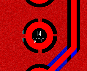 | 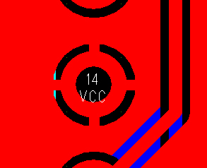 |
|---|---|
| With texturing on | With texturing off |
The Background Color swatch is used to set the background color for the display. By default it is black.
The Hi-Contrast Color swatch specifies the color to draw the current layer while in Hi-Contrast mode.
The Lo-Contrast Color swatch is used to specify the color to draw all objects not on the current layer while in Hi-Contrast mode.
The Ratsnest Color swatch specifies the color to draw ratsnest lines (connections yet to be made).
The Pin Names Color swatch is used to specify the color to draw pin names in. It can be invisible.
The Net Names Color swatch is used to specify the color to draw net names in. It can be invisible. Net names only appear inside of pads and vias and then only if they fit.
The Object Colors swatches are not really a global setting but rather provide an easy way to set the color of a class of objects regardless of what layer they are on.
User Preferences Layer Colors Page
The User Preferences Dialog is invoked from the View/User Preferences menu item. The Layer Colors Tab contains per-layer color settings. When this dialog is invoked all the settings are obtained from the currently active design. You can load a new set of preferences from disk, save the existing settings to disk, reset them factory defaults, or save the settings as the new defaults.

All the Layer Color swatches control the color of all objects on their respective layers. Setting the color of a layer sets the color of all object types for that layer.
User Preferences Routing and Spacing Rules Page
The User Preferences Dialog is invoked from the View/User Preferences menu item. The Routing and Spacing Rules Tab contains settings for the autorouter and for design rule checking. When this dialog is invoked all the settings are obtained from the currently active design. You can load a new set of preferences from disk, save the existing settings to disk, reset them factory defaults, or save the settings as the new defaults.

The Global Minimum Spacing – All Layers field allows you to set the minimum spacing for all layers at once.
The Per-Layer Minimum Spacing fields allow you specify the minimum spacing on a per-layer basis. On high volume boards you may want to increase the spacing on the outer, solderable layers while employing less restrictive spacing on the inner layers for additional routing channels.
The Routing Grid field controls the granularity by which the autorouter attempts to find paths. The finer the routing grid the denser the routing will be at the expense of time and possibly area. The area restriction will most likely be removed in a future release.
The Via Bias drop list controls how liberally the autorouter will use vias while searching for paths. The possible values are:
Use Freely – The autorouter will meander very little on a layer, enforcing a very strict horizontal/vertical layer direction. This is useful if the design has plenty of room for vias but poor ‘flow’ the layout where an excessive amount of meandering may block too many channels.
Neutral – This is the default for the autorouter. It does a reasonable job of reducing via count while maintaining decent layer directionality.
Avoid Using – The autorouter will attempt to meander around objects rather than move to a different layer with a via. This can prove fruitful when there is minimal room for vias.
No Vias – The autorouter will not attempt to use vias at all. It will basically attempt to route the board as a series of single-sided boards.
The Autorouter Layer Bias drop lists allow you to set up layer preferences or even restrict the router from using some layers altogether. The possible values are:
Favored – The autorouter will attempt to use this layer (and others with the same setting) before any other layer.
Neutral – This is the default. The autorouter neither prefers nor avoids this layer.
Avoid – The autorouter will only use this layer if it absolutely necessary to complete a path.
Do Not Use – The autorouter will not attempt to use this layer at all. This does not prevent a via from passing through this layer. You can route a single layer board by setting all layers except one to this value and instructing the router not to use vias.
The Autorouter Layer Direction drop lists control the preferred layer direction for each layer. The possible values are:
Horizontal – The autorouter will route on this layer in a horizontal direction.
Any – The autorouter will meander in any direction on this layer.
Vertical – The autorouter will route on this layer in a vertical direction.
Zoom To Coordinate Dialog
The Zoom to Coordinates dialog is invoked by pressing the ‘X’ key in the Design or Edit Footprint view. It is used to center the viewport on a specific coordinate.

The Enter Coordinate field is initially defaulted to the current gridded cursor location at the time of invocation. Enter the X and Y coordinates you desire in the format of your choice. The coordinates can be separated by spaces or commas.

