Schematic User Guide
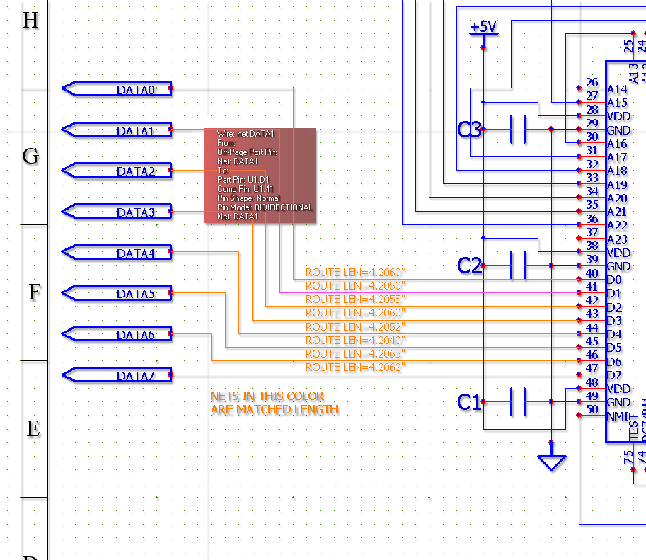
The Schematic/PCB Contract
A little background
PCB123’s purpose is to create a win-win situation for all parties. Customers download the free software and use it to design their products with a guarantee that, so long as they stay within the system parameters, the PCB’s will work as designed.
Because the software is developed and maintained on site, Sunstone can continually assess and react both to the customer’s needs and to its own internal needs. The business model has allowed a somewhat non-traditional approach to CAD software development. Because revenue derives from the use of the software and not the sale of the software, less emphasis is placed on software features and more on software throughput. We do not have to beat some competitor by providing a larger bullet list of esoteric features than the other vendor just to make a sale, but we do have to ensure that everyone from a novice to an expert can get through their designs to press the Order button. Because we know who will be processing and manufacturing the design (us) we can make certain assumptions where it might simplify the design process for PCB123 users.
This is all wonderful but there comes a point at which we (Sunstone) have to decide how far to take it. The software cannot outpace our manufacturing capabilities, and because customer support is free, we try to refrain from adding low-use features that clutter the software for novices or complex features that are deemed likely to generate a high volume of calls for instructions. There are both good and bad aspects to this method. An example is the autoplacer tool; the only interface to it is the ‘Run Autoplace’ menu item. If you can click on a menu then you have met the threshold required to use it. This is simple for you and results in predictably less support needed by us. We could expose many of the internal settings that would precisely control the autoplacer, but we know the performance gain that you may realize is too small to justify all the support calls that a dialog box with a bunch of strange settings would generate. Instead, we carefully pick the best values for the most typical boards. Either running the tool will help you, or you select Undo. Unless we can provide a set of options that will affect some major change in strategy, then it would probably not be fair to expose you to something that may burn your time trying to get some last magic adjustment to what is supposed to be a tool for “roughing in” an initial component placement. Win-win is the goal.
Generally, software that we develop will have wide appeal, general use, or transparent behavior. The new Plug-in development environment was, in a way, developed as the ultimate general use feature and a way forward for developing those esoteric tools that you may desire. You can write tools yourself, and it will probably be just a matter of time before a tool development community forms around the SDK.
This does not mean we aim at the lowest common denominator. In fact, it is just the opposite. Because our goals are different from those of a traditional CAD vendor, we sometimes arrive at solutions to problems that are quite different from the “traditional” way.
PCB123 Version 5 is a direct result of looking at the problem from a different angle. We know why customers will use the schematic; they will use it with the goal of creating PCB’s. Nothing was done to preclude the addition of simulators later on, but by admitting that we were creating a schematic capture tool as a front-end for PCB design, we have allowed ourselves to color outside the lines of tradition and see if maybe there is a better way to do the task.
Until now, PCB123 shipped a schematic capture application that was a third-party OEM product not directly developed or maintained by Sunstone. With every new release of PCB123, the schematic application fell behind in capabilities compared to the layout software. It also became a proportionally larger source of customer support issues. Serious consideration was given to just scrapping the schematic product, directing customers to freeware schematic applications and merely writing netlist importers for the layout software. The problem with that was our usage statistics did not support abandoning a schematic point tool – not everyone used PCB123 Schematic, but enough people did that we couldn’t just drop the functionality. The clincher was this: we could find no free schematic program that we were comfortable recommending.
And so it was decided that a new schematic program should be created in-house and that we should aim it at being highly PCB-centric and, keeping with the model, should take advantage wherever it could to increase throughput for customers.
We like win-win situations and it seemed to make sense that we create the schematic application right inside the PCB123 application. We would be able to leverage the existing software framework and users would not have to be flipping between applications.
This led to some deep questions about the traditional interface between a schematic and a PCB. With the two applications residing in the same framework, using a netlist for transferring data seemed to be a contrived solution. Why not have the PCB and schematic synchronized at all times? If both applications were tightly integrated, they could share so much more than a netlist.
For it to work, a couple of rules had to be established. They are simple, require no extra steps by you, the customer, and are largely automatic.
The Design-by-contract solution
Design-by-contract, as applied by PCB123, simply outlines a set of requirements that must be met before some operation can be completed. For instance, one requirement for placing a symbol on a schematic page is that the symbol must identify the PCB footprint that it uses. Otherwise, the PCB would not be able to synchronize with the schematic without complaining. Why allow a symbol that is missing critical data to be used? Why not provide the means for supplying the data either automatically or though low-pain facilities in the program?
Binding a footprint to a schematic symbol should perform the necessary checking to ensure the symbol pin numbers match the PCB footprint pin numbers.
Another rule for placing a symbol is that it must have a design-wide unique reference designator (component name). That rule is a perfect candidate for automating.
Notice above we only mention restricting the placement of a symbol instance with an incomplete or invalid symbol, we say nothing about the creation of one! So why allow a symbol to be created unless it fulfills a requirements contract? The answer to that is simple: some schematic symbols, such as a resistor, live up to their names and are completely symbolic. The same resistor symbol can be shared by many thousands of different parts that physically have various shapes and sizes. It would be ridiculous to have to create the same schematic resistor symbol for every different size resistor. Conversely, there are common chip packages that are shared by thousands of different chips, but each one may require a unique schematic symbol. An elegant solution to these problems was worked out so that the fulfillment of the symbol contract requirements happens even while providing the flexibility for symbol reuse. This will be covered in detail under Symbols and Parts.
All this talk of contracts and requirements may sound restrictive, but that is not the case. Most contract requirements, such as the unique reference designator requirement mentioned above, are automatically fulfilled by the software. The only time a requirement might bubble up as an action for the user are a couple of situations where the user would have to eventually resolve the problem anyway.
So far, we have only been talking about changes in the schematic initiating changes to the layout but the reverse must be accommodated too. Changes must be allowed to happen from both the schematic and the layout tool and synchronization should be bidirectional. It is reasonable to expect a component such as a decoupling capacitor to be added from within the layout tool. This operation requires that a schematic symbol representing the PCB component be added to the schematic in order for the two sides to match. The problem is, which symbol should it use? To expect that a PCB footprint would contain a reference to a schematic symbol for it to use does not even make sense. To accommodate this, a couple of services had to be created in the software.
The first service is a generic-symbol generator. At a minimum, it creates a rectangular symbol with a reference designator and one symbol pin for every package pin found in the footprint.
The other service needed by the software is the generation of special schematic pages called Sync pages. Parts added from Layout are automatically placed on sync pages. These are just like normal pages except they maintain internal bookkeeping for where to place the next auto-generated part. Connections between pins (edges in the graphs) are not mapped, nor need to be mapped between the PCB and the schematic but the nodes (pins) do. The main reason Sync pages are differentiated from regular pages is they are considered under system control. You should not manually add parts on these pages. Nothing dangerous should happen, it’s just that a future auto-generated part may be placed on top of your part.
 If a new connection is added to a pin in the PCB, then a Global port is added and attached to the pin in the schematic. This will happen on whatever page the pin is on, and is not limited to a sync page. Global ports are identical in operation to power and ground port symbols in that they expose a net name for global use. A picture of an automatically-generated symbol wired with global ports is shown to the left.
Besides detecting when new objects are added to the design, the software must also accommodate object deletions and modifications. Deletions are very straightforward, as nothing has to be synthesized or de-referenced. There is not necessarily a one-to-one correspondence between deleted objects from both sides. Deleting a component from Layout may result in several gates being deleted from the schematic. Conversely, deleting a gate from the schematic may not delete a component in the PCB if there are other gates from the same part still in use. The pins used by that gate will certainly be disconnected from any nets in the PCB.
There is a use case that you may have noticed and are worried about: If you want to perform a simple cosmetic operation such as cutting a circuit from one page and pasting it into another page in the schematic then this operation as described above would do catastrophic damage to the existing PCB layout. The moment the circuit was cut from the original page, all the components and routing in that circuit would be removed from the PCB. Then, when you added it back into the destination page all those parts and their connections would be added to the PCB at the system origin. Fortunately, PCB123 deals with this situation just fine. The only restriction is that the operation must be performed during a single session in the software. You cannot cut, then exit the software, or even close the design and expect it to paste successfully in a later session.
Special note: Some object modifications are not directly allowed. Luckily, these are rarely required. One example is you cannot simply change the footprint reference in an already-placed schematic symbol and expect a new footprint to be swapped into use for the corresponding PCB component. To perform this operation, you are forced to delete the old symbol and add it back in with a symbol that specifies the new footprint reference. This ensures that the contract requirements are satisfied in a standard order. If the part you wish to switch to is in the Library of parts you can switch the part out from the layout.
Go to the layout footprint, right click and select properties. On the components tab type in the new part name in the Part Name field and press tab. If the part name is found in the Libraries you will be prompted to update the selected part. If you have multiple parts that need to change to a specific part you can use Ctrl + click to select the group and use the steps listed above to update them. Using this workaround may change some wires to ports on the schematic side. These steps will update the symbol, footprint, and BOM entries with the new part information.
Properties
A property is a named piece of data. It is the most primitive type of object in the system and every type of schematic object in PCB123 can act as a container for an arbitrary amount of data in the form of properties. A property is either a user-defined property or a system-defined property. There is no difference between the two types of properties other than system-defined properties will be actively interpreted by the software.
The only restriction placed on a property name is that it must begin with a letter or underscore ‘_’, but property names that begin with an underscore are reserved for system-defined properties and should not be used for user-defined properties. Property names will always be converted to uppercase.
The value of a property is arbitrary. It may represent a color, a size, a picture, or anything else as long as it can be stored as a string of characters either directly or by some conversion. The character string can be any length except zero. Setting a property to empty has the effect of removing that property from the object that it is attached to.
Schematic objects have specific fields that are intrinsic to the object such as a location or rotation field in a text object. These fields are present in every instance of a text object. Objects may be specified with additional fields that are not intrinsic – they are essentially optional fields. It would be wasteful to store the font name and font size inside every text object that is displayed. It would be bothersome to change the font on every piece of text that stored it intrinsically. This is the reason system-defined properties exist. A system-defined property such as _TEXTFONT can be attached to a text object to specifically set the font to use when displaying that piece of text. If the property is not present, then some default is used. Let’s look at how that default is chosen.
Properties exhibit ‘bubbling’ behavior. What this means is that if a property value is requested from an object and that object does not contain the requested property, then it will forward that request ‘up’ to its parent and so on. Let’s look at a simplified diagram of the parent-child relationship of a part placed on a schematic page.
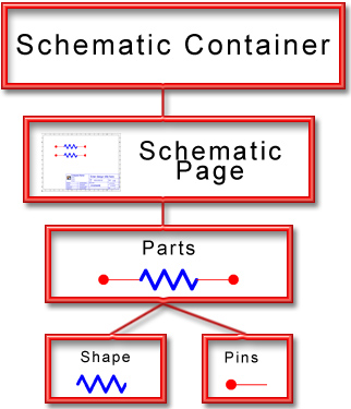 The picture to the right shows that a top-level object called the Schematic Container is the parent of schematic pages, which in turn contain children such as parts. A part can be a container for shapes and pins (among other things).
Attached to the schematic container is a default value for every system property. They act as a sink for property value requests that are not honored by child items. When the system attempts to draw some shape that is owned by a part, such as the resistor shape on the left, then a request for the _LINECOLOR property is made of the shape. If the shape contains a _LINECOLOR property that is set to green, then the search ends and the line will be drawn in green. If the shape didn’t have a _LINECOLOR property, the request is forwarded up to the parent of the shape which is a part. If the part had a _LINECOLOR property set to purple, then that becomes the default line color used to draw all shapes owned by the part that do not specify a _LINECOLOR property. When objects are created, they will use the default values for many of the various system-defined properties by simply not defining the property for the object. This means you can change the value of a single property such as _TEXTFONT in the top-level schematic object and all text will use that font when being drawn unless specifically overridden in an object.
There are numerous system-defined properties. Most are accessible through the Properties Dialog by clicking on this  icon from the various context panes it appears on, or by right clicking on an object and selecting properties. In most cases you do not have to deal directly with the property names but rather their descriptions and many have context sensitive controls such as a color popup if the property value is a color.
Some properties are read only. In these cases, they will be displayed in gray and cannot be changed. What use is a read-only property? The answer to that is you can add Text objects that display the value of a property instead of a static text string. That means a text object can be created that displays the value of the _NUMPAGES property even though that property is a system-managed value. This will be covered in detail later on.
Symbols and Parts
This section describes the relationship between symbols, sections, parts, footprints, and components.
Wow! That was a mouthful. Isn’t this supposed to be a simpler system? The answer is yes, but allowances have been made to accommodate a high degree of structure, and that in turn can aid efficiency and increase productivity.
Designing an electronic circuit has traditionally been graphical in nature where the electronic components used in the circuit were represented by symbols and their interconnections by lines, or “wires”, drawn between the symbols. Today, many circuits are designed in text editors using structured languages such as Verilog, VHDL, and C/C++. But that’s if the circuit being designed resides in a chip. Using that chip in a product still entails hooking it up to the rest of the circuit using a graphical schematic.
When drawn on paper, a schematic can play fast and loose with the level of detail required to convey the circuit’s intent. Historically, most symbols didn’t need specific pin numbers or pin names and many didn’t even indicate reference designators -- only a value or a part number.
An electronic version of a schematic is a different story. The reason schematics are drawn using special schematic capture software is to corral a great deal of information for use by other software programs such as digital simulators, SPICE simulators, and PCB design systems. The schematic software also generates BOM (Bill of Materials) reports, various statistical reports, and even performs simple semantic checking on the circuit.
Half the information contained in a schematic is the interconnection between components by drawn wires. These interconnects define their own data by where they are drawn or, more specifically, where they end. They describe the interconnection by conductors (edges) between component pins (nodes). In graph theory, a set of connected nodes is called a network but the ECAD industry has shortened it to just net. So there it is: half the information in a schematic is the interconnection of components by connecting networks of pins with wires. If the other half of the information in a schematic were so simple, you would only have one more paragraph to read.
Unlike wires, the other half of the information doesn’t describe itself. Luckily, the great majority of the information is contained in the reusable symbols and parts, which are stored in a library. The rest of the information is design-specific and most of that is auto-generated.
So what is the other half of the information? The simple answer is part data. A part is more than just a symbol plopped down on a schematic page.
A Part is assembled from various entities that reside in libraries. The relationship between these libraries is as follows:

The part library is a searchable database of parts organized in a flexible hierarchy. It accommodates the reuse of both schematic symbols and PCB footprints by allowing one library object to participate in many different parts. It is described in detail below.
Schematic symbols are created in the Symbol Editor and are saved either into the standard symbol library named std.sym, or into a custom library that you created.
PCB Footprints are created in the Footprint Editor and are saved either into the standard footprint library named Std.slb or into a custom footprint library that you created.
The single best reason for creating custom symbol and footprint libraries is because the standard libraries may get overridden during software updates. Sunstone reserves the right to grow the standard libraries from release to release.
The Parts Data is copied in its entirety from the libraries and into a design. Once an object is loaded into a design, it becomes fully encapsulated and travels with the design file (does not require that the library file be present to work with the design.)
If you wish to copy libraries from one machine to another, then you need to know where they are. The root directory for all library files will be Windows XP: Documents and Settings\All Users\Application Data\PCB123\Lib or Windows 7/8 Programdata\PCB123\Lib on the system drive. This directory may be hidden from you but the PCB123 installer should have installed a link named PCB123 Files in your My Documents folder. The link points to the Windows XP: Documents and Settings\All Users\Application Data\PCB123 or Windows 7/8 Programdata\PCB123 directory. Clicking on it will browse to that directory. From there, you will see the Lib subdirectory. Any custom library that you create will be created in the Lib\Custom subdirectory.
Parts
A part is typically an electronic component that is purchased and mounted to a PCB. A part has a logical manifestation and a physical manifestation. The physical manifestation is a single instance of a PCB footprint that contains the pad geometries and/or drill hole locations for mounting and soldering the part on the PCB. The logical manifestation of a part consists of one or more graphic symbols instantiated on a schematic page or pages. The reason a part may have several schematic symbols is due to some logical or functional partitioning of the part. PCB123 has adopted the term Section for each partition but you may also think of them as gates.
| Class | Prefix | Symbol |
|---|---|---|
| Battery | B |  |
| Capacitor | C |  or or  |
| Diode | D, or CR |  |
| Fuse | F |  |
| Connector | J, or P |  |
| Relay | K |  |
| Inductor | L, or FB (Ferrite Bead) |  |
| Transistor | Q, or VR (Regulator) |  |
| Resistor | R, or RN (Network) |  |
| Switch | S, or SW |  |
| Transformer | T |  |
| IC or Chip | U |  |
| Crystal | Y, XTAL, OSC |  |
| Zener Diode | Z, or D, or CR |  |
A part has a name called a reference designator that is unique throughout an entire design. The reference designator consists of an alpha prefix and a numerical value. In addition, each section of a multi-section part will have an alpha suffix that is unique to each section of the part. You have total freedom to specify the alpha prefix but the numerical value and possible suffix are managed by the PCB123 software.
There are standard prefixes for different part classes such as resistors and capacitors. The table on the left lists the most common part classes along with the prefixes and a typical schematic symbol for that class.
You have the ability to assign a prefix to a symbol. All parts that use that symbol will have that reference designator prefix.
Besides a reference designator, one or more symbols, and a PCB footprint specification, parts may contain other information such as a value, tolerance, manufacturer’s part number or distributor number such as a Digikey catalog number. In reality, a part may hold any information you desire. How this extra information is acquired will be described shortly.
Please refer to the back of this manual for up-to-date information on the naming conventions employed by the Accelerated Designs Ultralib parts available for use in PCB123 V5.
For now, let’s move on to the role a symbol plays in a part description.
Symbols
A schematic symbol is a collection of primitive objects such as pins, 2-D shapes, and text that are treated as a single entity and may represent a complete part or one section of a part. Symbols reside in libraries, where they may be referenced by parts.
Some symbols, such as resistors and capacitors, are highly generic and a single symbol may be suitable to represent thousands of different parts. Other symbols, such as an MCU, may be created that are unique to just one part. There are even some symbols that are never intended to represent a part at all but only sections of a part, such as a NAND gate.
There are no hard rules, but in general the more specific a symbol is to a particular device, the more information you want to bind to it. Conversely, a symbol that will be used for a large assortment of parts will want to stay reasonably generic in the information it specifies.
Symbols can be drawn by hand using the Symbol Editor or they can be created automatically with the Part Wizard. Symbols created automatically with the Part Wizard are limited to a rectangular symbol with pins that can be described in spreadsheet fashion.
Symbol text
 Symbols may contain both static and dynamic text objects. Intrinsic to a text object is a string to display. How that string is interpreted depends on the text type. If it is static text, then the string is displayed verbatim and does not change unless a new string is supplied. Dynamic text will interpret the string as the name of a property (system-defined or user-defined) and display the bubbled value for the property name. The symbol on the left is a highly-generic symbol that has two dynamic strings. When this symbol is incorporated into a part and that part is placed on a page, then the _REFDES will be replaced with the actual reference designator for the part and _PARTNUMMFG will be replaced with the manufacturer’s part number if supplied to the part.
Other intrinsic text fields besides the string include:
Text Location - The X,Y coordinate for the text origin. The Y origin is always at the top of the character cell but the X origin depends on the text alignment described below.
Text Rotation - Either 0 degrees (horizontal text) or 90 degrees for vertical text.
Text Alignment - Specifies either Left, Center, or Right aligned text. The X origin for the text will coincide with the left edge, center, or right edge of the text respectively.
The following system-defined properties may be used to affect the display of text objects:
_TEXTFONT - Specifies the font name to use when drawing the text.
_TEXTSIZE - Specifies the text height in points. There are 72 points in one inch.
_TEXTCOLOR - Specifies the color of the text. This is usually set with a color picker but in the event you gain textual access to this property, you can encode the Red, Green, and Blue values using the following formula: color = (Red*65536)+(Green*256)+Blue, where each color may range between 0 and 255. Additionally, you may set a color to invisible by setting it to (or adding) 2,147,483,648.
Symbol shapes
You can add lines, arcs, and regions to symbols. Virtually every display characteristic for shapes are controlled by attaching system-defined properties to the shape or, to specify them all at once, attaching the property to the symbol. The system-defined properties that affect the display of shapes are:
_LINEWIDTH – Specifies the width of the line. This is typically selected from a choice but numerically it is in 100ths of an inch (10 1/100ths of an inch = .1 inches)
_LINECOLOR - Specifies the color of the line or outline.
_LINESTYLE - 0 = solid, 1 = dashed, 2 = dotted, 3 = dot-dashed.
_FILLCOLOR1 - Color to fill the interior of closed regions.
_FILLSTYLE - 0 = hollow, 1 = solid, 2 = horizontal hatched, 3 = diagonal hatched, 4 = cross hatched, 5 = diamond hatched.
Symbol pins
Probably the most important primitive that is included in a symbol is a pin. Pins map a logical port on the symbol to a physical pin in the footprint. Pins have a hotspot (designated by a small, solid circle) that provides a tie point for wires.
Graphically, A symbol contains an inside and an outside. The smallest the inside can be is the rectangle that bounds all drawn shapes in the symbol. Pins will be constrained to the edge of this rectangle and will always face outward. This provides uniform alignment of the pins and ensures the automatic wire router has a clean escape from the pins without bumping into shapes.
Intrinsic to pins are:
Internal pin name – A label for the pin. A pin name must be supplied for a pin. It is recommended that the names be unique within the symbol but it is not required. This relaxed rule is to accommodate multiple names such as GND or VCC in a symbol or part. If a pin name ends with 2 hyphens, or minus signs (‘—‘) , then the hyphens will not be displayed, but rather a bar will be drawn over the pin name. This is a visual indicator for “NOT”, or inverted.
External pin number – The pin number of the footprint this pin represents. When creating a generic symbol that may be used by different footprints, it is not necessary to define a pin number, as shown in the symbol above. Generic symbols are expected to be assembled into a part using the Part Wizard. By the time a symbol is used in a part, it must have acquired a unique pin number for every pin and the pin number must match a pin in the footprint. The double-hyphen mnemonic does not apply to pin numbers because they have to match up with the name of a footprint pin. They are called pin numbers but may in fact contain other characters than digits.
Pin shape – There are several graphical styles that pin can assume. They are:
 | Zero Pin | Zero-length pin. Not typically used. |
|---|---|---|
 | Normal Pin | No special meaning attributed to pin. |
 | Dot Pin | Signifies and inverted state. |
 | Clock Pin | Indicates pin is used to clock the device. |
 | Dot-Clock Pin | Inverted clock. |
Pin Type – Classifies the pin’s function. Assigning a pin type to a pin allows that pin to participate in certain rules checking such as the Electrical Rules Check. This check will catch wiring combinations that are suspect such as a GND pin tied to a VCC pin. Possible values are:
N/C - Pin is never connected.
VCC - Pin is tied to voltage source.
GND - Pin is tied to ground.
PASSIVE - Default pin type.
INPUT - Pin is an input to an active device.
OUTPUT - Pin is an output from an active device.
BIDIRECTIONAL - Active input or output pin.
TRISTATE - Pin may assume high impedance state.
ECL - Emitter-coupled logic.
Pins will always snap to an immutable pin grid. This, coupled with a symbol rotation restriction of 90-degree increments ensures that pins will always stay on a neat grid.
The only active system-defined properties for pins are _PINNAMEVIS and _PINNUMVIS. When these properties are set to zero, the pin name and pin number respectively will not be displayed.
In the future, pins may contain properties that both drive and probe a simulator.
Symbol properties
Recall that in the discussion of symbol text we used as an example a system-defined property named _PARTNUMMFG. In that discussion we showed how a dynamic text whose string value was set to _PARTNUMMFG would display the manufacturers part number if it found one. So where would it find this value? If we wanted, we could add a property called _PARTNUMMFG to the symbol itself and set its value to SN74AHCT00N just as an example. When it was time to display the text object, it would bubble up a request for the value of a property named _PARTNUMMFG and would get back SN74AHCT00N almost right away. The fastest answer would be if it contained the named property itself. Because the text object didn’t possess that particular property, it forwarded the request up to its parent, which is the symbol itself. In this example symbol (the NAND gate pictured above) it wouldn’t make much sense to bind such explicit information to the symbol. After all, we want to use that symbol wherever we can to avoid duplicating effort. So the symbol is not a good place to store device-specific properties if the symbol is intended for reuse. That doesn’t mean it can’t contain other useful properties.
One such property is the reference designator prefix, which in this case would always be ‘U’. Now you wouldn’t have to specify it using a property because there is a dedicated place to fill in that information but behind the scenes, the symbol editor is actually binding the reference designator prefix to the symbol in the form of a property. Even on a symbol that just represents a gate and not a part, this property will find a home because when a part object is assembled from one or more symbols, the part will suck up any properties that were specified by the symbol.
 In fact, if we specified just one more property we could automatically create a part object that could be placed on a schematic page. Take a look at the symbol on the left. It is a single-sourced relay that is available in only one package size.
Because this is most likely a one-off symbol, it makes sense to specify device-specific properties right in the symbol. There are a pair of system-defined properties named _PARTFOOTPRINT and _PARTFOOTPRINTLIB. By specifying these properties right in the symbol, PCB123 will have all the information it needs to instantiate the symbol directly on a schematic page.
In fact, this is not what happens. PCB123 actually creates a part object and assembles all the necessary information automatically. Again, you do not have to specify the properties directly because the symbol editor has a very handy graphical footprint browser and search tool. You can just click on a footprint to use and it will automatically create and bind the footprint properties. In addition, when you save the symbol to a library, it will perform full validation on the pin number mappings and only save the symbol if it completes the contract terms. It will also add an entry into the part taxonomy so the symbol can be searched in the normal way. It adds an entry under the “Generic Symbols” family of the “Other” part class in the taxonomy. You can move it to a more orderly place if you desire.
So, we have seen how we can quickly flash up some pins and shapes in the symbol editor and then graphically browse for the footprint the symbol will use. After saving the symbol there will now be a part in the taxonomy that is immediately available for use.

We should back up just a minute and address the other scenario that we glossed over and that is how best to create generic symbols and then use them in parts with part-specific properties.
The picture to the left shows a pin assignment diagram for a Texas Instruments 7400 Quad NAND Gate. There is an inner rectangle showing the 4 NAND gates inside the chip and the small outer rectangles represent the physical pins on the part. The bold numbers are the pin numbers of the package and the small labels are the internal pin names. In this case, there is a pattern where the two inputs of each gate are named A and B, and the output is named Y.
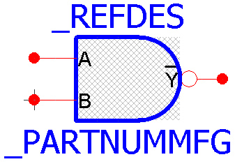
Let’s look again at our NAND gate. This symbol seems to have all the things we need if we want to place the NAND gates individually. It has the 3 pins and their names are labeled correctly. It has placeholders for values we want to see on the schematic page. So, let’s just see what part numbers this gate can be used in. We know it can be used in a 7400 part but that’s just a generic name for the part. We would have a difficult time ordering a part number 7400 from Texas Instruments. Here is just a sampling of the actual 7400 devices from various logic families.
SN7400N, SN74S00N, SN74LS00N, SN74HC00N, SN74HC00E, SN74HCT00N, SN74HCT00E, SN74AS00N, SN74ALS00AN, SN74AHC00N, SN74AHCT00N, SN74AC00N…
There are similar series for the 7401, 7403, 7424, 7426, 37, 38,…. 74804, 748003, all using the NAND gate and that’s just from Texas Instruments. Many of the parts where we would like to use the NAND symbol have widely varying configurations. Many have the same pin assignments but use different packages such as through-hole or surface mount packages, and still other parts have different pin configurations or even differ in the number of gates in a part.
With a little bit of organizing, we will be able to reuse the NAND symbol in hundreds of parts and decorate the parts with a rich information model.
The first step is to review the candidates and organize them by the number of gates in a part and the pin assignments for each gate in the part. A quick check of the TI data book shows that in addition to the 7400, the 7403, 7426, 7437, and 7438 series devices all share the same configuration.
Now that we have identified the gate and pin assignments that are needed, you will use the Symbol Editor, go to Tools > Symbol Editor.
You will use the tool bar across the top of the symbol editor to create and edit your symbol.
New Symbol – Use this to start a new symbol.
Open Symbol – Use this to load and existing symbol for editing in section A.
Save – Save your symbol
Cut – Cut the selected object
Copy – Copy the selected object
Paste – Paste the selected object
Undo - Last operation
Redo – Last operation
New Section – Add an additional section to your symbol
Delete Section – Remove the currently selected section of your symbol. Never delete section A.
Select Object – Allows you select any object in your symbol
Add Pin – Add pins to your symbol
Add Line – Add a line to your symbol
Add Rectangle – Draw Rectangles
Add Polyline – Draw polylines
Add Polygon – Draw polygons
Add Arc – Draw Arcs
Add Circle – Draw circles
Add Text – Insert Text
Add Image – Insert Image
Description of Zoom Toolbar
Zoom In
Zoom Out
Zoom All
Refresh
Actual Size
Change Grid
½ Active Grid
Double Active Grid
Select the Open Symbol button on the toolbar to load an existing symbol. If you do not want to use an existing symbol, you can begin drawing your symbol here. You will draw the body of your symbol in the shaded area provided using the polygon tools. Place your mouse near the edge or at a corner of the shaded area left click and hold, then move your mouse to change the size of the shaded area. The area will always be rectangular and the pins of your symbol will lie along the perimeter of this shape. You can use the Add Pin tool to add each terminal.

Search for the symbol you would like to start with in Step 1. Select the symbol in Step 2 and then select Load Symbol in Step 3.

If you would like to load an existing symbol to an additional section, use the Add Existing button. You can create a new blank section by selecting the Add New button. Use the Remove button to delete the selected section.

Once a new section is added, you see a tab labeled B and the pin numbers are updated. You can toggle between the tabs to edit each section.

Add section C by selecting Add Existing as described previously. You could also select Add New to create a blank section. Then copy the contents of section B into the newly created section C. When you copy and paste into the new section you may need to adjust the shaded area to fit correctly around the symbol.
In section C, the copied pins are labeled seven, eight, and nine. In the 7400 pins, 7 and 14 are hidden so you must edit the pin numbers. Select the pins tab to edit the pin numbers.

Change the pin number for section C to eight, nine, and ten. Start by changing pin nine since duplicate pin numbers are not allowed.
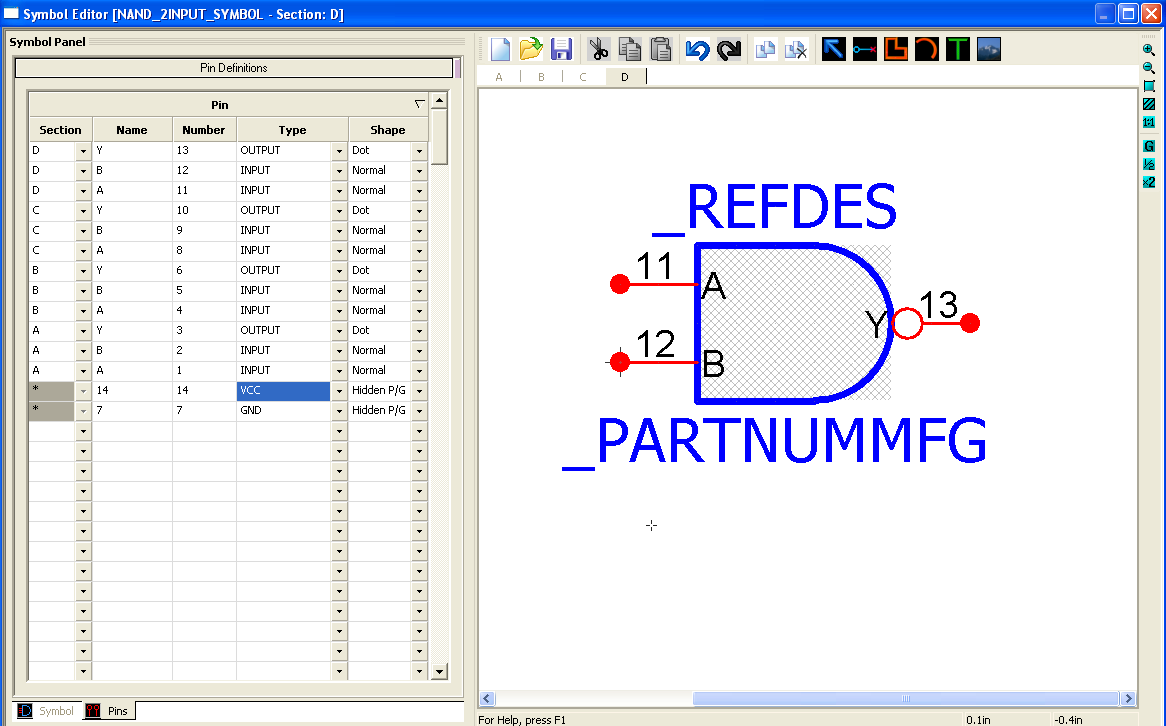
Switch back to the Symbol tab and add Section D as described previously. Once you have all four sections of this symbol in place select, the pins tab to edit the pin properties and add the hidden pins.

On the pins tab modify the pin properties as shown below.

You will add pin 7 by clicking in the first empty Number field and type a 7. Select the shape Hidden P/G type GND and change the Name. Repeat for pin 14.

You can change the Section, Name, Number, Type and Shape of each pin. Use the drop down menu for Section, Type and Shape. Double click in the Name and Number fields to edit. As you make changes to a pin, you can see the changes in the preview window. As changes are made on the pins tab, you can move pins as needed in the preview window.
After updating the information on the Pin Definitions tab, review each section and use the Save icon to save the symbol. Please save custom symbols to a new library. The libraries included with the PCB123 download cannot be used to save your custom parts.
Save the part into our library using the generic name QUAD_NAND and select OK.
Remember, all we have done to this point is create a template to be used by a large number of different parts. Nowhere in this exercise did we specify an orderable part number, nor did we bind the template to any physical footprint.
Binding templates to create library parts is accomplished using another toolset inside PCB123 and will be discussed in the next section, The Part Taxonomy.
Pre-Defined Parts
With PCB123 V5, Sunstone Circuits is proud to include an extensive library of 750,000+ commonly used parts and connectors. These parts definitions are sourced from Accelerated Designs Inc., in Huntsville Alabama, and are drawn from the Accelerated Designs Ultralib product. These parts are fully defined and available for use by PCB123 users. Parts definitions include:
Schematic Symbols (multi-part where applicable)
Footprint
Reference Designator
Parametric data including:
Values
Manufacturer Name
Manufacturer Part Number
DigiKey Part Number
Hyperlinked part data sheet
Hyperlink to the Digi-Key product summary page
As we’ve already mentioned in this section, a 750,000 parts library would require huge amounts of storage and create unworkable download times. Furthermore, the average PCB designer uses about 20,000 parts in their personal library. Trouble is, not every engineer uses the same 20,000 parts. To this end, PCB123 makes the entire catalog available as an online web service. Users search for parts by the functional parameters, and select them from the search results. If the part is not currently local to the user’s taxonomy, PCB123 can download the ADI Ultralib family in which that part is defined. In this way, users dynamically fill out their taxonomy based on the parts they regularly use, and avoid making room for the 730,000 or so parts they’ll never use.
PCB123 and Accelerated Designs do not expect that we’ve defined every part you will need. It is our expectation, however, that these library parts will greatly reduce the amount of time spent by users in defining parts. Furthermore, with standardized parts available, users can have the peace of mind that they are referencing known-good parts definitions.
Finally, the Accelerated Design parts all contain appropriate manufacturer and Digi-Key part numbers (wherever possible). These part numbers enable LiveBOM queries inside the Bill of Materials tab. So not only do you have access to a fully defined schematic and footprint symbol but, thanks to LiveBOM, you can also check for availability, pricing and second source information via the Digi-Key website.
For more information about the structure, organization and naming conventions employed by the Ultralib parts, please refer to the back of this manual.
The Part Libraries
Sunstone examined various schematic capture programs during the development of the new schematics facility in PCB123. We looked not so much at the features of these systems, but how they managed design processes. One thing that stood out was how dissimilar the various systems were in how they dealt with libraries and managed parts. Surprisingly, the places where they did agree we didn’t necessarily think were the best solutions to the problem. Sunstone walked away from the evaluations more with a list of what not to do than of features to emulate. This is not a knock on those systems. After all, they paved the way to make the comparisons possible.
Searching for a part was another issue. Most of the systems we evaluated based their search criteria on the name of a part. Systems that provided capabilities beyond that typically did so by drilling down through additional dialog boxes that offered up different search criteria. None of the systems we evaluated allowed an arbitrary search term, such as a resistor value, to be entered in a general search that successfully found a part. We were of the opinion that the name of a part was almost irrelevant unless maybe it was a manufacturer’s part number or something that was universally known. With some parts, it does not even make sense that you would key off the name when selecting it. For instance, if you need a resistor then you should be able to type 4.99k, 1% and get a list of parts that include those criteria. You could guide the search more specifically by entering 4.99k, 1%, 1/8W, Rohm, or by entering a specific manufacturer’s part number.
Something that is always fun to play when developing a new product is the “wouldn’t it be neat if…” game, such as “wouldn’t it be neat if we included an entire catalog of parts, such as the DigiKey catalog, with the system?” Well yes, it would, and if we could create 1000 parts a day, and there were approximately 750,000 parts in the catalog, then it would take 750 days to complete. This clearly precludes the creation of a catalog library from the initial release. Even so, we must be sure the system is capable of handling such a large library for future releases that just might contain such a catalog. A library containing half a million or a million parts would be massive. Each part would include not only a catalog number and manufacturer’s information, but also any number of properties that could be useful as searchable criteria or as parameters for tools such as simulators.
Another problem with such a large library is creating it! We went to great pains to describe how the symbol editor and the part wizard may be used to create generic symbols and part templates. If the symbol library only contained a single resistor symbol, and the footprint library only contained a handful of resistor footprints such as the standard 0402, 0603, 0805, and 1206… sizes, we could still create parts for about 20,000 manufacturer or catalog parts numbers. Each part would proclaim, “I am such and such part. I am manufactured by company X as part number Y, and I can be purchased from this catalog as catalog number Z. I use this schematic symbol and this PCB footprint. Some of my important characteristics are….”
Something like that could almost be done in a spreadsheet, as shown below:
| Mfg. | Mfg. # | Cat. # | Symbol | Footprint | Value | Tol. | Power | V Max |
|---|---|---|---|---|---|---|---|---|
| Rohm | MCR10EZHF17.8K | RHM17.8KCCT-ND | RESISTOR | RC0805L | 17.8K | 1% | 1/8W | 150V |
| Rohm | MCR10EZHF18.0K | RHM18.0KCCT-ND | RESISTOR | RC0805L | 18.0K | 1% | 1/8W | 150V |
| Rohm | MCR10EZHF18.2K | RHM18.2KCCT-ND | RESISTOR | RC0805L | 18.2K | 1% | 1/8W | 150V |
| Rohm | MCR10EZHF18.7K | RHM18.7KCCT-ND | RESISTOR | RC0805L | 18.7K | 1% | 1/8W | 150V |
| Rohm | MCR10EZHF19.1K | RHM19.1KCCT-ND | RESISTOR | RC0805L | 19.1K | 1% | 1/8W | 150V |
| Rohm | MCR10EZHF19.6K | RHM19.6KCCT-ND | RESISTOR | RC0805L | 19.6K | 1% | 1/8W | 150V |
| Rohm | MCR10EZHF20.0K | RHM20.0KCCT-ND | RESISTOR | RC0805L | 20.0K | 1% | 1/8W | 150V |
| Rohm | MCR10EZHF20.5K | RHM20.5KCCT-ND | RESISTOR | RC0805L | 20.5K | 1% | 1/8W | 150V |
That would be great because spreadsheets lend themselves beautifully to automation or tabular processing. The only problem is that some of the columns shown in the table above will not work for any part types other than a resistor, and even then, it might be missing columns that are important to you such as temperature stability or RoHS compliance.
There is something interesting to observe with this table; each row defines a part but nowhere does it specify a name for the part. What is its name? The answer is, who cares? If each row specifies all the necessary information for a part, including how to purchase one, then we don’t care what it is called, as long as we can find it in a search. That is what we mean by part names being contrived entities and why we did not want to rely on them for searches.
You could point PCB123 to any one row and it could assemble a part for placement on a schematic page. In fact, every column in the table could be removed except the Symbol and Footprint columns and PCB123 could assemble a part for placement. With all the other columns, PCB123 creates a property that uses the column name for the property name and the cell value for the property value.
This is where the payoff happens by keeping symbol definitions generic if there is any hint that they can be reused. A search for a part can be performed using any criteria and all the matches (read choices) will be presented to you. You can then select your choice and the software will bring in the referenced schematic symbol and the referenced footprint, perform all the necessary validation, and if everything is fine, it can then create a part instance, give it a reference designator, and add all the other columns of data to the part in the form of properties. Later, when you want to generate a bill of materials, it may include such items as a catalog number and quantity for each part type which you can then send to the part distributor. Even better, it puts PCB123 on the cusp of automating the purchase of your PC boards, the part kits, and even assembly services just by pressing the Order button. It’s too bad we didn’t have a Sell Product button too!
Getting back to the table shown above, careful observation shows that only three out of the nine columns have varying data. That is a lot of redundant data. In addition, we still have not addressed the fact that the table is only good for specifying resistors, and that is not even indicated anywhere. Luckily, there is a neat way to solve both problems.
Hierarchy and Inheritance
A Part, in the library, is just a collection of properties. They are the leaves in the hierarchical tree structure and may contain no children.
Besides the list of properties that a part may explicitly define, it also inherits all properties that its parent family and any ancestor thereof may define. This is how the redundant data from the table above is removed. In fact, this data “folding” is a natural way to define a hierarchy for a part. To do this, we set two goals: the first is that all parts in a family have the same number of properties (columns). The second is there should be no column whose every value is the same. If we find a column with invariant data, then it should become a property of the parent and the column removed by deleting the property from all the child instances.
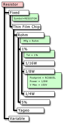
 If we were starting from scratch, all we would have is the part classes as shown on the left. We know the table represents resistors so the Resistor part class is where we will start defining or discovering the hierarchy for the table.
 First, we check if there are any invariant columns to eliminate by adding a property to the parent, in this case the Resistor part class. The closest candidate would be the Symbol column with its value RESISTOR but that might be asking too much of the Resistor part class because there are other resistor symbols such as a variable resistor. This indicates the need for a subspecies to differentiate between at least fixed resistors and variable resistors. We will create two families called Fixed and Variable, but we will only be concerned with the Fixed family for our purposes.
 To the Fixed family, we will assign a property named Symbol the value RESISTOR, as shown to the right. This will assign the RESISTOR symbol to any child family and part under the Resistor\Fixed family and we can remove the Symbol column from the table.
With our active node being the Fixed family, we again look at the table and determine there are no more invariant columns that we can safely eliminate by adding additional properties to the Fixed node. A good check for this is by asking the question “are all…?”, as in “are all fixed resistors made by Rohm?”, or “are all fixed resistors 1/8W?” If the answer is no, then the column must be eliminated with further refinement.
 Families do not have to be limited to just the invariant columns in the table. In fact, we will add another family named Thick Film Chip under the Fixed family, but we will not add any properties to it that we know of yet.
The only way we can eliminate another invariant column is to further refine the hierarchy with another family. This is a subjective process, but in this case, it seems to make sense to refine by manufacturer, so we will create a family named Rohm and assign to it a property named Mfg whose value is also Rohm. This is shown at left.
We can then eliminate the Mfg column from the table and proceed in the same fashion for the additional invariant columns.
The image below shows what the family hierarchy looks like after all invariant columns have been eliminated. The table now contains only 3 columns, all of which have variable data.
| Mfg. # | Cat. # | Value |
|---|---|---|
| MCR10EZHF17.8K | RHM17.8KCCT-ND | 17.8K |
| MCR10EZHF18.0K | RHM18.0KCCT-ND | 18.0K |
| MCR10EZHF18.2K | RHM18.2KCCT-ND | 18.2K |
| MCR10EZHF18.7K | RHM18.7KCCT-ND | 18.7K |
| MCR10EZHF19.1K | RHM19.1KCCT-ND | 19.1K |
| MCR10EZHF19.6K | RHM19.6KCCT-ND | 19.6K |
| MCR10EZHF20.0K | RHM20.0KCCT-ND | 20.0K |
| MCR10EZHF20.5K | RHM20.5KCCT-ND | 20.5K |
These are our parts and they will be added to the Resistor\Fixed\Thin Film Chip\Rohm\1%\1/8W family, and each will contain a Mfg #, Cat #, and Value property as shown below.
| Property Name | Property Value |
|---|---|
| Mfg # | MCR10EZHF17.8K |
| Cat # | RHM17.8KCCT-ND |
| Value | 17.8K |
Those three properties are what is stored for each of the potentially thousands and thousands of fixed resistor parts. However, because of inheritance, when a query for a part is made the set of properties returned is usually more than just what is bound to a specific part. The returned list is called the effective properties for the part.
here is an example of the list of effective properties returned due to inheritance:
| Property Name | Property Value |
|---|---|
| Mfg # | MCR10EZHF17.8K |
| Cat # | RHM17.8KCCT-ND |
| Value | 17.8K |
| V Max | 150V |
| Power | 1/8W |
| Tol. | 1% |
| Mfg. | Rohm |
| Symbol | Resistor |
| Footprint | RC0805L |
You can see we pick up a substantial amount of nearly free data including the all-important symbol and footprint bindings.
Before we proceed, we need to make a small clarification. What is shown as the Symbol property and the Footprint property are simplifications for clarity. The primary tool used to edit the taxonomy, which is called the Part Manager, actually provides graphical browsers to select the symbol and footprint for these properties. In reality, the browsers add two properties each. Symbol is actually two properties named SymName and SymLib. Footprint is actually FpName and FpLib. The library names are needed to fully resolve the location of a symbol or footprint.
Additionally, the Part Manager’s interface includes several built-in property names to encourage their use. We have been used Mfg #, Cat #, Value, Tol, and Mfg in the above example, but in reality these property names are system-defined property names that map to:
| Example Name | System-defined Property |
|---|---|
| Mfg # | _PARTNUMMFG |
| Cat # | _PARTNUMDIGIKEY |
| Value | _PARTVALUE |
| Tol | _PARTTOL |
| Mfg | _PARTMFG |
Typically, you will not have to deal with these names because there is a user interface to deal with them. We just wanted to make you aware that not all the columns are as general as we have led on in the spirit of clarity. The above properties do in fact want to map to their specific system-defined property names because PCB123 will make great use of them.
Pre-defined Parts

With the current release of PCB123, Sunstone has included an extensive updated parts library from Accelerated Designs in Hunstville, Alabama. PCB123 had included 750,000 of the most commonly used parts, and optimized this list to support parts currently orderable in the Digi-Key catalog.
The initial installation of PCB123 will include a library file that contains the search criteria for all of the new parts, as well as full part definitions for the NXP parts library and generic parts. Because 750,000 parts can be a very large database, Sunstone has placed the complete parts database on a secure web server. To access the parts, users merely perform parameter searches, then select their part from the returned search results. If the selected part has not been copied to local storage, then PCB123 will prompt the user to initiate a parts family download.

When the download is completed, users will see the following dialogs. At this point, the parts family containing the selected part will be loaded to the user’s local parts storage. In this way, users’ individual needs will evolve the parts maintained locally.
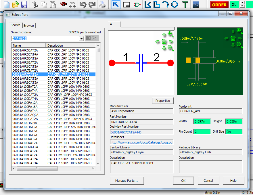
Once the user returns to the parts selection dialog, shown here, the selected part will be fully loaded into the window.
Select OK, and you will be returned to the schematic edit window, with the selected component attached to the cursor for placement.
If you Find a Problem with a Pre-defined Part
Sunstone Circuits provides online and live technical support for PCB123 at no cost. If you find a problem with a part in the Accelerated Designs Ultra Lib library, you can email the following information to support@sunstone.com:
Part Name
Library Name
Description of the issue/problem
A screenshot if possible
Sunstone Circuits and Accelerated Designs will then research and resolve the issue.
The Part Manager
If you create a generic symbol – a symbol without a footprint binding, no default entry will be created in the part taxonomy because it is considered “incomplete” for use in a schematic. There is no rule against adding an incomplete part to the library but it is assumed that generic symbols will never be intentionally used as is. It is assumed you will create specific bindings to footprints using the Part Manager.

While in the schematic editor, the Part Manager may be invoked at any time from the Display Panel by pressing the Manage Parts button. The Part Manager dialog is split into a left side and a right side as pictured below. In this example, we have drilled down into the Resistor part class, and through several Part Families to select an individual part in the tree on the left. The effective properties for the part are displayed in the grid on the right side. The properties displayed in red are inherited from the ancestors of the part, and the properties displayed in black are assigned directly to the part.
When you select and item this way, you may add, delete, or modify the properties of that item. If you click on a different item after changing the properties, the changes will be applied to the selected item before changing to the new selection.

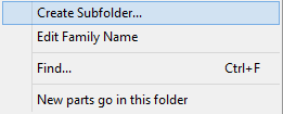 If you right-click on either Part Class items or Family items, you will be presented with a popup menu that allows you to perform several commands. Create Subfolder allows you to add structure to the Libraries as you see fit. Families may be added under the root part classes and under other families. You may select Edit Family Name, or just click on a family label two times to engage in-place editing of a family name.
Find allows you to search the taxonomy. New Parts go in this folder allows you to select a folder to store newly created parts. Left click on a folder to select it then right click and select New Parts go in this folder. Selecting the Create Part button will automatically store new parts in the selected folder.
Fill in the Properties shown in the center of the screen. The only required field in this section is Manufacturer’s Part Number. Next use the Select Symbol and Select Footprint buttons to load the symbol and footprint for your taxonomy entry. You may also want to add more properties to your part. Go to the properties section and select the property name under the Name column then enter the appropriate value under the Value column. After entering all of the required part information select Create New Part to store the part in the taxonomy. If you want to modify an existing taxonomy entry select the part, edit the desired properties then select Apply Changes.
Acquiring Data
There are two primary ways to acquire the data in PCB123 V5. One is to locate the part you seek in the PCB123 version of Accelerated Designs’ Ultralib parts library. This is essentially a function of a parameter search inside the part library, followed by a potential part family download from the Sunstone server location. Alternatively, if the part you seek is not currently defined in the Ultralib, you can create the part yourself.
Finding the Part in The Ultralibs Library
In PCB123 V5, users can search for parts using parametric data, from either the schematic tabs or from the layout tab. When using the Schematic tab, just select the Select Part dialog box (shown here) and enter appropriate search criteria in the search box. Here you can see we searched for a “RES 0402 1.0K” which will return all parts that contain all these search terms. The resulting list contains a number of 0402 sized SMT resistors. Users can then select any of these resistors to view the schematic, footprint and parametric data. In this example, we’re looking a t a Yageo SMT from the Ultralibs parts.
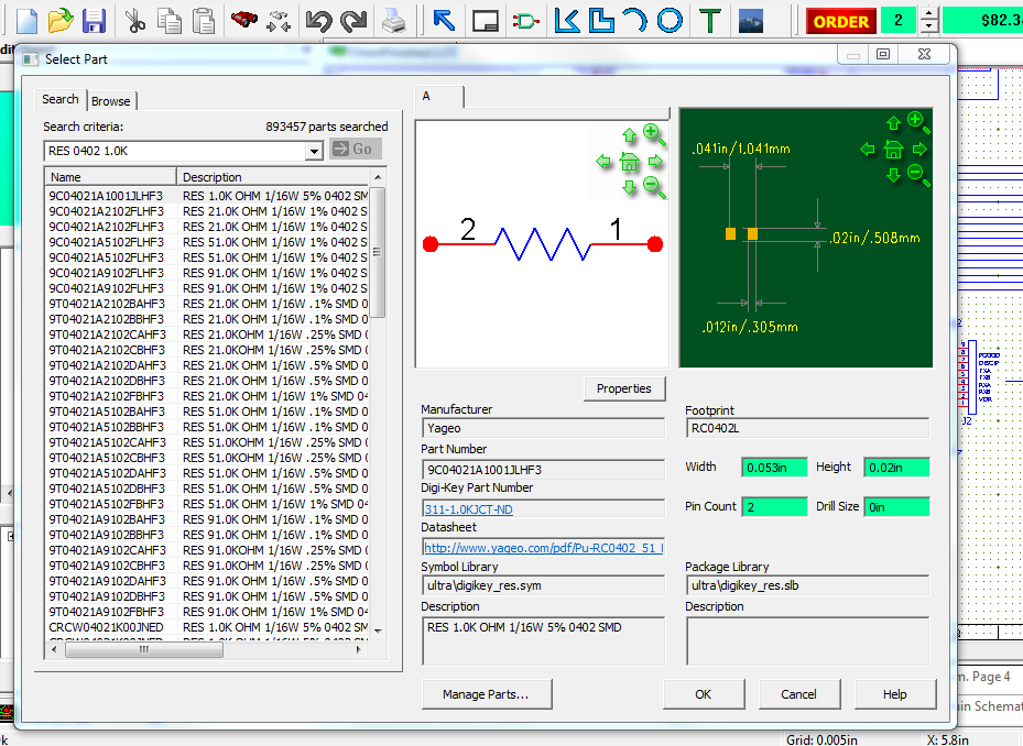
This part is representative of most of the Accelerated Designs parts definitions: the schematic side symbol is defined and meaningful; the footprint is complete and includes dimensional measurements to help the user confirm the part; below is a list of parametric data including:
Manufacturer
Part Number – this is the manufacturer’s part number
Digi-Key Part Number – the orderable part number from Digi-Key for this component.
Datasheet – a link to the manufacturer’s product data sheet. Useful for designers to either investigate a part more closely or to confirm the part performs as expected.
Symbol Library – where in the taxonomy does this part reside? Users can verify the source, whether the part comes from Accelerated Designs, from the PCB123 Generics, or from the user’s custom-built libraries.
Description – typically this field holds a parameter string comparable to that used in a Digi-Key component search.
Package Library – Location for the footprint symbol.
Width/Height – dimensions for the part’s physical packaging
Pin Count – number of pins for the package
Drill Size – for through-hole parts, the specified drill hole diameter for the part.
If this part suits your needs, just click the OK button and you will be returned to the schematic sheet and in part-placement mode, ready to include the part in your design. It’s that easy.
Each individual placement of this part then appears on the Bill of Materials tab, and the footprint is pre-placed on the layout’s origin, ready for placement and routing.
Creating the Part Yourself
Below is a sample of one part series from the Digikey catalog. It is a family of oscillators made by Citizen.
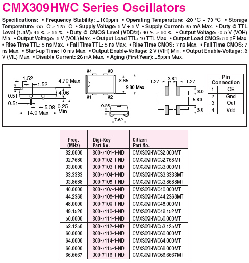
Using shorthand, we can create each part in the series all at once. The first thing we want to do is create a place in the library for them. Under the Crystal part class, we will create the following families:
Oscillators
Surface Mount
Citizen
CMX309HWC Series
After creating the families and sub-families, click on the Citizen family item and enter Citizen in the Part Manufacturer Field then select Apply Changes.
Now, in the taxonomy tree, select the family you just created named CMX309HWC Series. We will be able to bind a good deal of information to this item.
The information above shows a single package being used for all the parts in the series. We can click on the Value ellipsis for SymName and FpName to select the symbol and footprint this series will use. On the next empty row in the grid, select Part Tolerance from the list of system-defined properties and enter +/- 100ppm for its value.
Next, add the following custom properties to the grid, each one on a blank row:
| Name | Value |
|---|---|
| SUPPLY_VOLTAGE | 5V |
| SUPPLY_CURRENT | 35mA |
| NOMINAL_DUTY | 50% |
Select Apply Changes.
We are now ready to create the parts under the selected family. We are going  to “screen scrape” the information for the parts. Since many part specifications are PDF files, we will use the Adobe Acrobat Reader as the example program where we are viewing part data. Acrobat Reader has a tool called the Select tool whose icon is shown to the left.
Clicking this icon puts Reader in a mode that allows a block of text in the PDF to be selected and copied to the clipboard. This tool also has a secret mode that allows for columns of data to be selected. If you click on the beginning of the column you wish to copy and, while holding the Alt key down, drag to the end of the column, you can release the mouse button and you should see just that column highlighted. Press Ctrl+C or select Edit/Copy from the menu in Reader to copy that column to the clipboard. In our case, using the table above, we will column-select the values from the Freq.(Mhz) column taking care not to include the column title itself, and then press Ctrl+C to copy the values to the clipboard. You may want to paste the information to an Excel document to use later.
Back in PCB123, select the CMX309HWC Series item in the tree then select the Spreadsheet tab. Copy and paste the contents of the first row into the second row. This is the first instance of the parts you will create in this family. You can copy and paste each column of information from your data sheet into the appropriate column of the Spreadsheet tab. If you need to add more columns right click on an existing column label and select insert column. You can also delete or sort columns. Once the table data is complete you can select the Create/Update button then choose the CMX309HWC Series family and store your new parts. You will need to confirm each part because we have not yet assigned footprints and symbols to the taxonomy items.
Below is a picture of the newly created parts. The properties shown are for the selected new part. When you press Finish, the taxonomy is refreshed in the schematic editor.

The Symbol Editor
The symbol editor in PCB123 is a dialog box with a work area and a few toolbars, as shown below. The actual symbol editor is usually larger than the picture; it was compressed to fit on a page. The symbol editor is invoked from the Tools menu while in the schematic editor. Because it is a dialog box, no other work may proceed on a design until the symbol editor is dismissed.
The symbol editor does not interact with any design; it only interacts with schematic symbol libraries. When it is invoked, a new symbol containing a placeholder for a reference designator is created. You may either begin adding objects to this symbol or load a different symbol from a library into the editor.

Inside/Outside
You may have noticed the crosshatched rectangle in the work area in the above 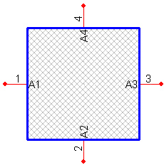 picture. This rectangle represents the interior portion of the symbol. Symbols are divided into an interior and exterior. Shapes will always reside in the interior of a symbol and pins always on the exterior, as shown to the left.
When adding pins, they will always be confined to the perimeter of the rectangle with the hotspot always pointing outwards.
If you draw a shape that extends outside the rectangle, the rectangle will be enlarged to encompass the shape. Any pins present on the sides that enlarge will move with the new rectangle. This is all done automatically for you.
 You may also change the size of the rectangle yourself. With the select tool
  active, you can move the cursor to any corner or edge of the rectangle to display drag handles, as shown at left. Clicking and dragging one of these handles allows you to adjust the size of the rectangle. The rectangle cannot shrink smaller than the shapes it contains.
Besides being constrained to the rectangle edges, pins will always be located on a fixed grid, called the unit grid. The size of this grid happens to be 0.1” and is immutable for pin placement. This restriction, coupled with symbol rotations restricted to 90° steps, ensures that all pins land on a uniform grid on a schematic page, which in turn ensures wires are drawn on a uniform grid.
The Wire Router also takes advantage of the inside/outside separation by not routing into the interior of any symbol, which in turn means it will not cross any lines of a symbol.
Text is under no such restrictions. It may be placed inside or outside the rectangle. The Wire Router currently ignores text and may route through it.
The working grid in the symbol editor may be adjusted either in half  by pressing the Minus key (-) or doubled
  by pressing the Plus key (+). This is only effective when drawing shapes or placing text. When placing pins the grid is always set to the unit grid.
Adding pins
Pictured below is the symbol editor as it appears with the Pin tool selected. It has been shrunk to view all the salient features in one picture. As soon as the Pin tool is selected, a new pin will be created that will track the cursor while staying constrained to the interior rectangle. As the pin is moved, it will snap to the unit grid and will automatically change orientation as it is moved to different edges of the rectangle.
While a pin is being moved, the Pin Attributes pane will be active on the left panel. It is here that you may fill out the information about the pin.
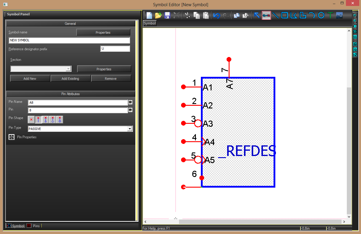
To release the pin at the desired location, just click the left mouse button. Adding pins is modal. When you left-click and place a pin, another one is created whose pin name and number are either auto-generated based on the last pin name or number, or they are obtained from a macro expansion. You must cancel out of the Add Pin mode by pressing the Esc key, selecting Cancel from the context menu, or selecting a different tool.
After creating two pins, a “stride” has been established that successive pins will add to the last pin location to derive a default location for the next pin. Both the pin and the cursor are snapped to this location allowing a whole row or column of pins to be quickly added by simply left-clicking without moving the mouse.
By default, the auto-generated pin name and number take the first sequence of digits from the previous pin name/pin number, and increment them by one. If no digits were present, it will change to the next letter in the alphabet.
At any time you may use bracketed shorthand notation in either the pin name field or the pin number field to establish a continuous sequence or a disjoint sequence of pin names and pin numbers to use for consecutive pins. The lifetime of the shorthand sequence is the duration of the pin tool being active. Once you cancel the pin tool, any remaining names in a shorthand sequence will be dropped.
A pin name and number must be supplied for a pin. If you are tempted to set a pin name or number to empty because you do not want it displayed, supply the name or number anyway and click on the eye icon  to the right of the field so it shows this
  icon. This sets the visibility of the pin name or number to invisible.
In the above picture, an example of each pin shape is shown. The pin shapes themselves carry no meaning in the software; they are merely added as a convenience so you do not have to draw the dot and clock symbolisms yourself.
Pin types do carry meaning in the software. The list of pin types forms a matrix of rules that specify which pin types are allowed to connect to other pin types. This is used during the automatic creation of wires when unconnected pins from two devices are placed on top of each other and during an Electrical Rules Check (Not yet implemented in this release). By default, a pin is assigned the Passive pin type that is allowed to connect to any other pin type except N/C pins. It is recommended that you supply a pin type for symbol pins if you have the correct information at hand.
Finally, the pin properties button  presents the standard Properties Dialog where you may specify any custom properties that you may wish to attach to a pin.
Adding Shapes
Pictured below is the symbol editor with the Shape tool selected. It also shows an outline shape and a filled shape that have already been created.
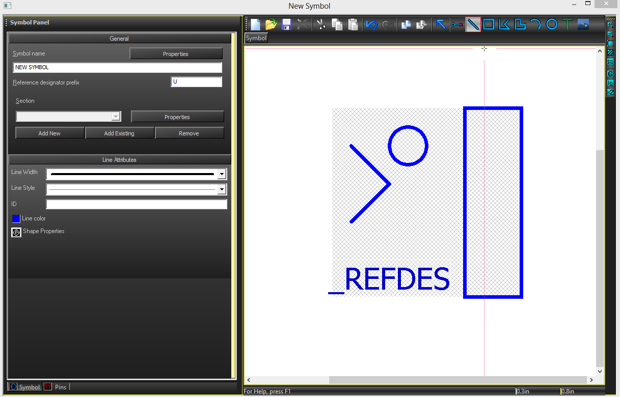
When a shape tool is selected, the symbol editor is placed in a mode where it is waiting for the first corner to be created by clicking anywhere in the work area. Once a corner has been created, a rubber band is drawn from the last corner to the current gridded cursor position. Clicking the left mouse button creates additional corners.
You can continuously “erase” the last segment by drawing back over the segment and clicking on the previous corner.
Finishing the shape can be done in two ways; the first way is to cancel or escape out of the mode and is the method to use when creating open polylines of one or more segments, or you can close the shape by creating the last corner at the same location as the first corner. This assumes there are at least 3 corners not in a line. Once finished, you are free to begin drawing another shape. Pressing escape or cancelling once again will put you back into the Select tool.
You may change the width or thickness of a shape outline by selecting one of the pre-defined line widths from the drop list in the Shapes attribute pane. These widths are provided for consistency. If a different width is required, you can specifically add a _LINEWIDTH property to the shape and set it to the desired value.
Another outline attribute you may change is the Line Style. By default, shapes use a solid line style. Other styles are dotted, dashed, and dot-dashed lines. Only the solid line style will display outlines in true thickness.
 The interior of a shape is controlled by the Fill Style attribute. By default, the fill style of a shape is hollow. The picture to the left shows the different fill styles available in the drop list. They are, in order from the top, Hollow, Solid, Horizontal Hatched, Vertical Hatched, Cross Hatched, and Diagonal Hatched. Selecting any fill style other than hollow will automatically close the shape if not already so.
The color of the outline and the shape interior may be independently set in the Shape Attributes pane.
Shapes may be assigned an ID. This can be any text string. The ID will play a role in upcoming releases as a means to programmatically identify shapes.
Finally, the Shape properties button  presents the standard Properties Dialog where you may specify any custom properties that you may wish to attach to a shape.
Adding Arcs
Pictured below is the symbol editor with the Arc tool selected. It shows an arc in the process of being created.
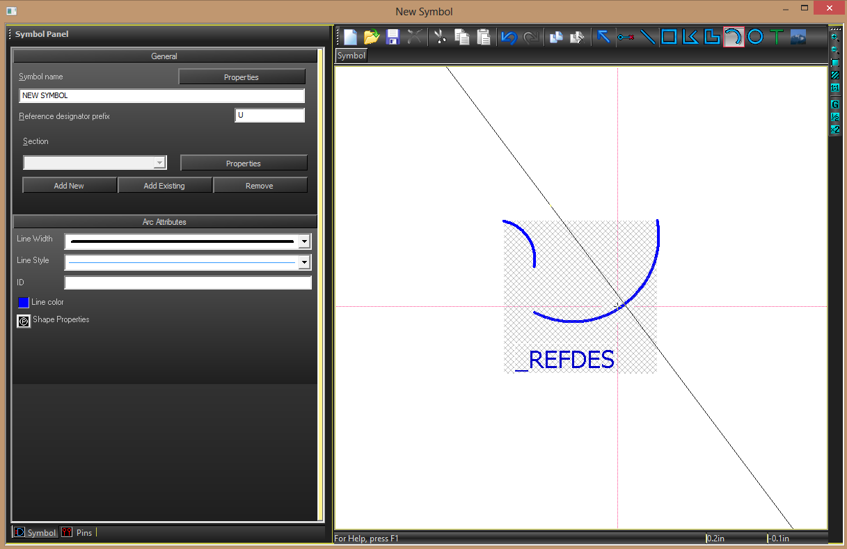
Creating an arc requires three clicks of the mouse. When the Arc tool is selected, the symbol editor is placed in a mode where it is waiting for the first click, which represents one end of the arc. The next click will be the other end, and the last click will be the arc apex. Once the first corner has been created, a rubber band is drawn showing the arc progress and a perpendicular guide is drawn showing the line upon which the apex may land.
The arc is automatically finished after the apex has been defined, and the symbol editor will be ready to create another one.
At any point during the arc creation, you may cancel or press the Esc key. Pressing escape or cancelling once again will put you back into the Select tool.
You may change the width or thickness of an arc by selecting one of the pre-defined line widths from the drop list in the Shapes attribute pane. These widths are provided for consistency. If a different width is required, you can specifically add a _LINEWIDTH property to the shape and set it to the desired value.
Another outline attribute you may change is the Line Style. By default, arcs use a solid line style. Other styles are dotted, dashed, and dot-dashed lines. Only the solid line style will display outlines in true thickness.
Currently, arcs have no interior. They are outline objects only. The color of an arc outline may be set in the Shape Attributes pane.
Finally, the Shape properties button  applies to arcs and presents the standard Properties Dialog where you may specify any custom properties that you may wish to attach to an arc.
Adding Text
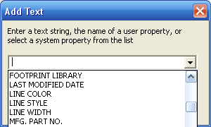 When you select the Insert Text tool, you will be immediately prompted for a text string to add using the dialog box shown below. If you have defined a user property with the same name as the string you enter here, the text string will be substituted with the value of the property. You may also expand the drop list to select the name of a system-defined property that will be substituted.
Once the string is defined, a text object will be attached to the cursor until you cancel or release the text string by left clicking.
After you place the text object, you will be prompted for another string. To exit either the dialog box or the Add Text Mode, press the Esc key or select cancel from a context menu.
The picture below shows the Symbol Editor while in Add Text mode.
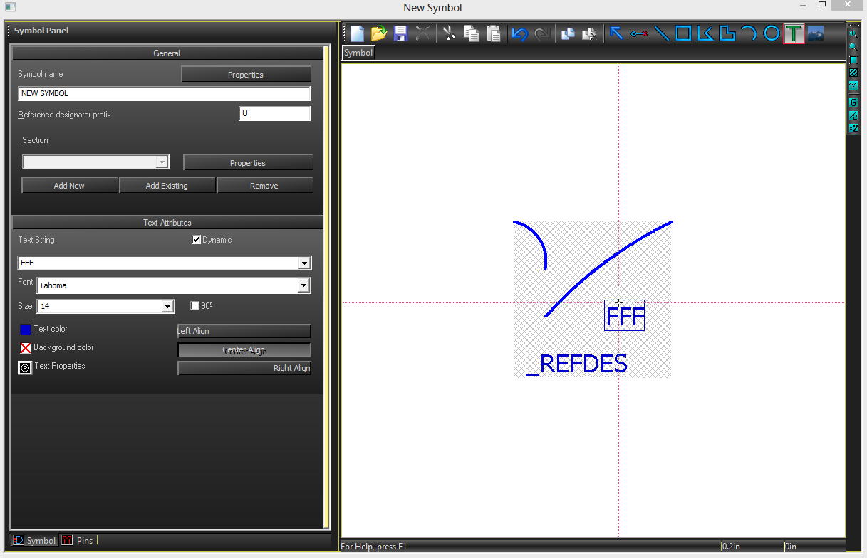
Text attributes can be changed as you define text strings. Attributes include changing: font size, rotation, text color, background color, and alignment.
Adding properties
To add a property to a symbol component, right mouse-click on the component and select Properties… from the context menu. The picture below shows the Properties dialog for a pin in the symbol editor.

Users can select from the list of predefined properties, or create user-defined custom properties. Clicking OK stores the property on the property list for the symbol component.
Saving symbols
 Click the SAVE icon in the Symbol Editor to save the symbol to the taxonomy. The picture below shows the Save Symbol dialog box. The Save Symbol dialog box contains three fields you must specify to complete the save process.
The Name of the Symbol will be the identifying name the symbol will use. Be descriptive.
The Description is a text field in which you can describe the symbol in more detail.
Parts Library, customer\generics.sym by default, is the library location to which the part symbol will be saved. There is also a New Library… button to allow you the ability to create a new custom library on-the-fly for your newly designed symbol.
Sections
You can schematically represent a single layout footprint with a symbol comprised of several sections. This is often done to represent the various gates of a particular component. To add additional sections select the “Add New” button. If you want to add a new section with an existing symbol select the “Add Existing” button. If you need to remove a section select the “Remove” button. You can change the letter shown under section to view and edit any of the sections you have added or created.
Binding to specific symbols
The process of binding together a schematic symbol (or set of sections) and a layout footprint happens in the Define Part dialog (shown in the figure below)
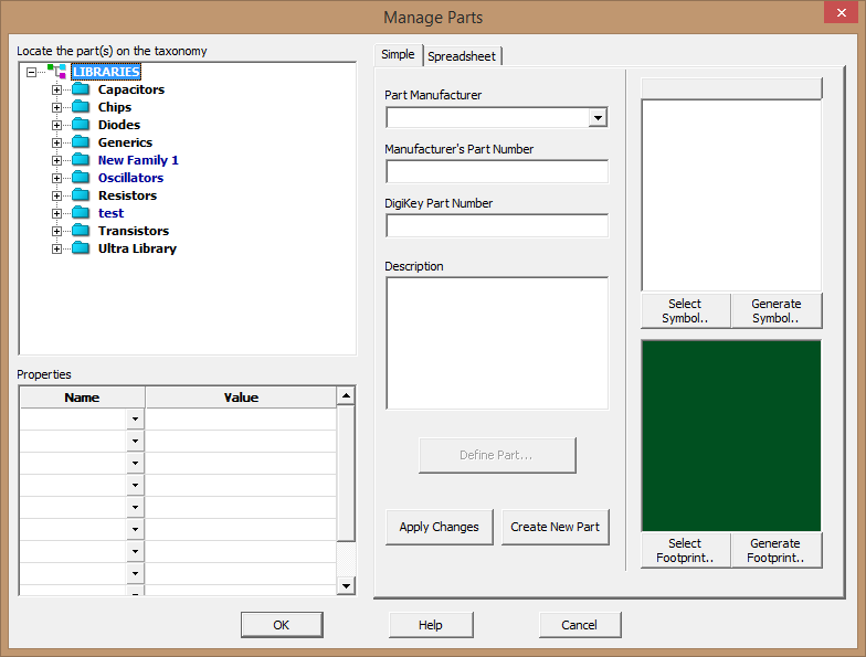
If you have already defined, or located, suitable symbols for schematic and footprint, you can quickly bind them together here.
Schematic Symbol – click on Select Symbol… navigate to the schematic symbol, and select it. The schematic symbol appears in the schematic symbol preview window
Footprint - click on Select Footprint… navigate to the footprint and select it. The footprint appears in the footprint preview window.
Specify the part meta-data, part manufacturer, manufacturer part number, DigiKey Part number and a description, then select Create New Part
If you wish to update the properties or symbols to an existing part, you can do that too. Just navigate the library to your part, then select it to load it into the Manage Parts dialog. Make the necessary changes, then select Apply Changes (instead of Create New Part) and submit your updates to the part definition.
Mapping pin names to pin numbers
Using the Symbol Editor in PCB123 V5 it’s easy to map pin names to pin numbers. In this figure (below) the assignment of pin names and numbers can easily be changed on the fly. Just click on the appropriate text box for the pin number of the pin name, and replace the existing value with the new value.
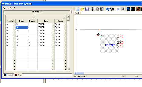
Pin numbers can be in non-sequential order, pin names can be functional. Each pin number must be unique to the part, but pin names can be duplicated as needed.
Hidden pins
Hidden pins are often used to provide power and ground connections to components, but not clutter the schematic views with all the power related routing.

 By clicking on the Pins tab at the bottom of the Symbol Editor pane, you can access the Pin properties table, as shown in the figure above. The Shape column allows users to specify a number of pin configurations, including Hidden P/G.
Once a pin is hidden, the pin structure for that pin disappears from the symbol graphics. The pin, however, is still present in the part definition.
A hidden pin is required to be identified as either a power or a ground pin. You will not be allowed to save your component until each hidden pin is so designated. To specify the type for the hidden pins, select the appropriate setting from the choices in the Type column pull down menu.
Saving parts
When you are ready to save your part to a library, select the SAVE function  from the toolbar.
 The SAVE function gives you access to the Save Symbol dialog, as shown in the figure above. Enter your name for the new symbol, an optional description, then the symbol (.sym) library to which the part will be added. If you need to create a new library, use the New Library… button on the dialog box.
Finding Parts
In PCB123, locating schematic parts for use in your design falls into two primary methodologies: Searching and Browsing.
Searching: You enter search criteria; PCB123 filters the entire domain of available parts to match your search criteria. The PCB123 search mechanism is quite flexible, using a generally free-form text search that scans properties, property values, and part names for text string matches.
Browsing: allows you to click-navigate the taxonomy to find appropriate parts.
Further details for both methods of finding schematic parts can be highly effective, depending upon what you need at the time.
Part search
Searching for parts by search criteria is highly effective when you know one or more key parameters for the part you require.
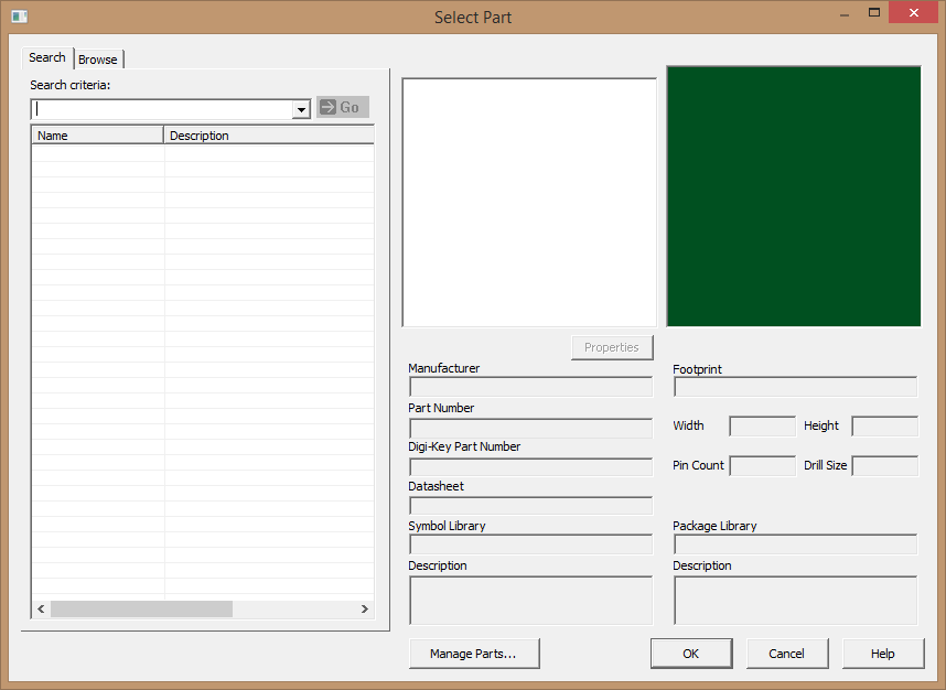
Just type the parameters into the Search Criteria field, and the Select Part dialog filters the parts list down to the existing parts containing that criteria.
When browsing for parts, the taxonomy representation comes into play. As shown in the figure below, users can browse through the hierarchical folder structure interactively until locating the desired part.
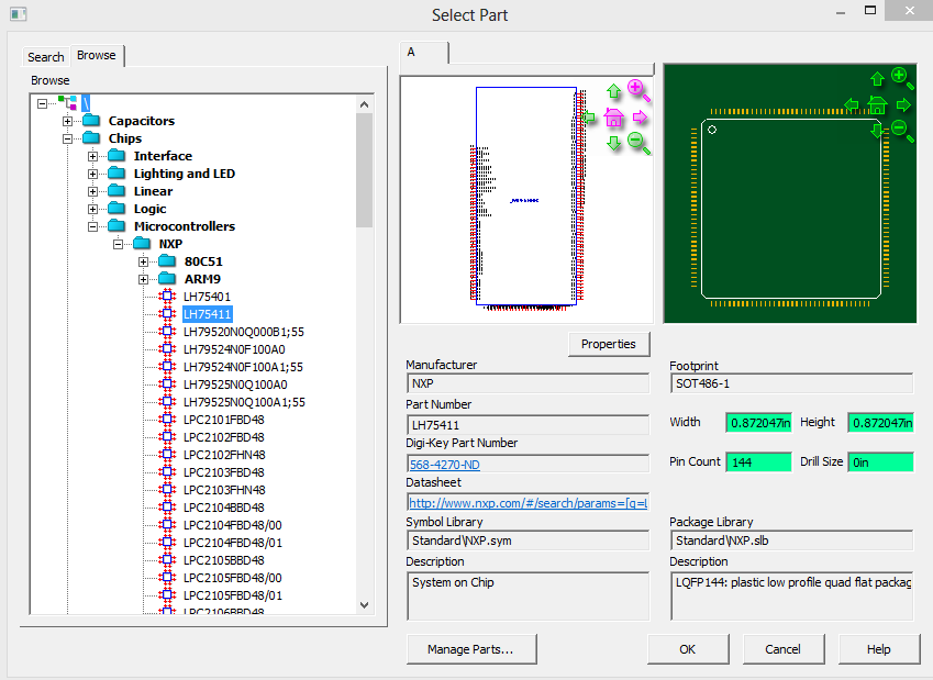
If, in either case, the user cannot locate a predefined part to suit the specific design needs, the next step may be to build a new part from scratch.
Define New Part
The Manage Parts button at the bottom of the Select Part dialog starts the new part definition process. Clicking the Manage Parts button takes you to the Manage Part dialog, shown below. The Manage Part dialog is quite powerful and flexible in how it approaches parts definitions. The key parts of the Define Part dialog include:
The Parts Libraries pane
The Properties definition table
The Simple Tab for component specification
The Spreadsheet Tab for advanced component specification
The symbol pane, showing the assigned symbol graphics
The footprint pane, showing the assigned layout graphics.

Whether you’re putting together a collection of pre-existing symbols to configure a new part, or whether you’re building everything from scratch, you’ll probably want to start by locating the library destination for the part before you do anything else.
In the figure below, the user is creating a subfolder in the library to hold the soon-to-be-designed component definitions. The context menu in this figure comes from right-clicking the mouse on an entry in the taxonomy window. Right-Clicking in this manner provides access to a number of commands for editing, organizing and modifying the taxonomy and its components.
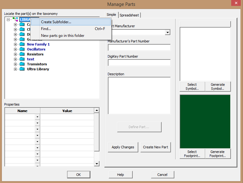
Once the taxonomy location has been identified, the next step is to fill in the Manufacturer information, manufacturer part number, and Digi-Key part number, if known. Users can also provide a free-text description of the component in the Description field. Notice that, as the part number information is filled out, a property entry for that information is automatically added to the Properties table in the lower left corner of the Define Part dialog.
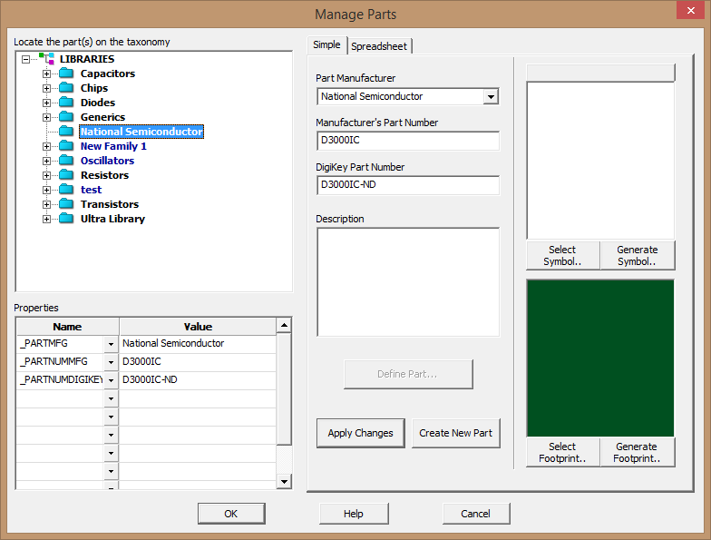
Next up, is binding symbols and footprints to the part definition. Starting with the schematic symbol, the user has two choices: Select a Symbol, or Generate a Symbol.
Selecting a symbol presents the user with a search dialog, as shown below. Locate the symbol of your choice, using search parameters.
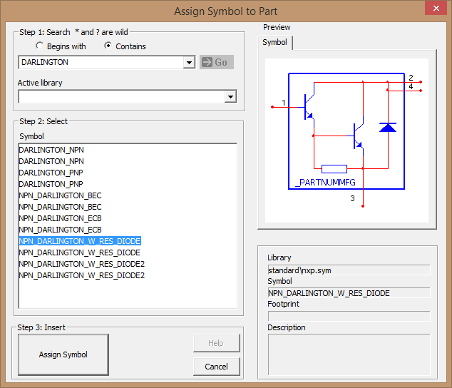
Once located, click on the Assign Symbol button to bind the schematic symbol to the part definition, resulting in a Define Part dialog that shows the newly bound schematic symbol.
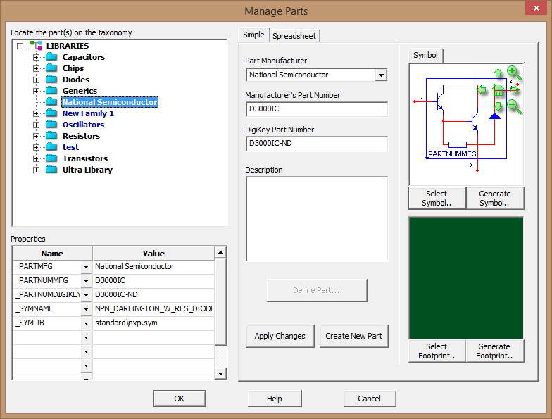
Now, bind the footprint. Like selecting the schematic symbol, users have two choices: Select a footprint, or Generate a footprint.
Selecting a footprint presents the user with this Select Footprint dialog.
Following a usage model similar to the schematic selection process, In step one, users can search for a component by parameter, or browse the footprint libraries using the taxonomy-like view in the lower left corner of the dialog box. In step two, you select the footprint that matches the component you have under definition. For step three, click the Select button in the center left. The figure below shows a Select Footprint dialog box ready for the binding process.

At this point, we’ve created a fully defined part. The figure below shows how the Define Part dialog box might look after binding both the schematic symbol and the footprint.

Click Create New Part, and reconfirm the location in the taxonomy. Once the part has been created, it appears in the taxonomy pane:
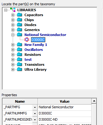
When you click OK on the Manage Parts dialog, you will be returned to the Select Part dialog (where this all started). Now, you will notice that your newly created part is available for use in the Select Part taxonomy, as shown below.

Select your part, and click the OK button. Your part is now ready to be placed in your design’s schematic. The figure below shows the part ready for placement.
 [superimposed on]
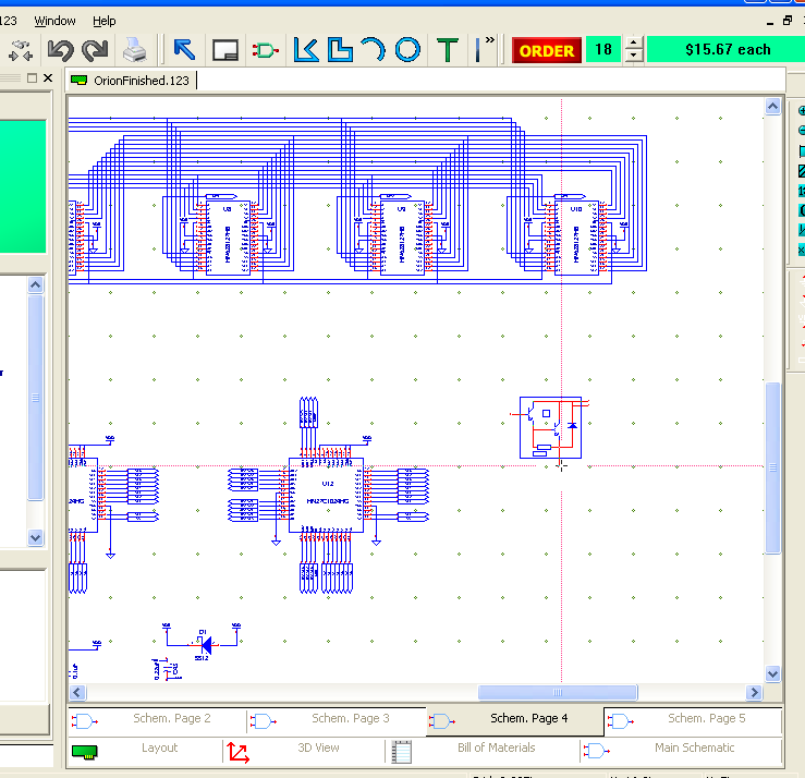
Ports
A port is used to add a net label to pin, wire or group of connections on the schematic. Ports can be used to make connections between pins without connecting the pins with a wire. Ports can also be used to make connections between schematic pages.
PCB123 provides you with an AGND, DGND, Voltage, Global and Off-Page port. The labels for the AGND and DGND ports can be changed. You can select a port from the menu bar by selecting Insert > Add Port. A port toolbar is also included on the far right side of the screen.
Ports and net names
After selecting either the Voltage GND, DGND, Global or Off-Page port you can change the net name assigned to it. You should see the Edit Panel in the on the left side of the screen. If you do not see the edit panel select View > Toolbars > Edit Panel. Start by selecting the desired port. Next, go to the top section of the edit panel. It should now show the label Net Name(s). Type in the desired net label in the Net Name(s) field then place the port and connect it to a pin or wire. If you have already placed a port, and wish to change the assigned net, then left-click on the port to select it. You will now see the Net Name(s) section in the Edit Panel. Update the text in the Net Name(s) field and place the port. When you place the port you will see the message “Do you want to rename all ports ‘Net Name’ to ‘NewNetName’?” If you select Yes, all ports of net named NetName will be changed to NewNetName. If you select No, only the selected port will change to the new net name.
Schematic Pages
PCB123 can support multi-page schematic designs, allowing you to create logical sub-designs to manage the complexity of the schematic design.

Adding Schematic Pages
To add a new, blank sheet to your design project, click the Add Page item on the Toolbar (highlighted below) and a new, blank schematic sheet will be added to your design. The default name for the new sheet will be “New Page”. A Schematic title block will also be attached to the new sheet.
 [superimposed on]
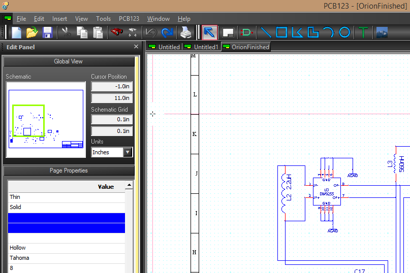
Synchronization pages
A Synchronization page is a special type of schematic page used to capture ad hoc symbols created for footprints not defined on the schematic side.
The Title Block
The Display tab contains the page properties and provides fields for updating the title block.
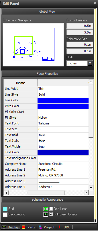
Page size
To set the page size for a schematic sheet, right click in the schematic pane. Select the Set Page Size… command from the Context commands, below.
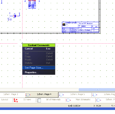
The page size is specified by individual sheets. Your multi-page schematic design can accommodate multiple page sizes at the same time.
The Schematic Editor
PCB123 allows you to design your schematic and simultaneously populate your layout with the parts in your design. By default, each PCB123 design file contains a minimum of one associated schematic page, labeled as Main Schematic. In the Main Schematic tab you will find all the tools to locate, create, place and connect all the components that will comprise your board.
To begin working in the schematic go through the new board wizard or create a new project. Look to the bottom of the screen and click on the Main Schematic Tab.
Adding parts to a page
Upon opening the Main Schematic tab you should see the Display tab within the Edit Panel. (If you cannot view the Edit Panel, choose View>Toolbars>Edit Panel). Select the Parts Tab to view the PCB123 libraries. Here in the libraries you are able to drill down into one of the folders that organize parts, such as Generics>Chips>Dips in order to find all of the available generic symbols for dual inline packages. You can simply double click on the part you wish to place then click on the schematic to place it. This provides a quick way to sort through available symbols by category.
You can also right click on any folder in the parts libraries and choose Find to search for particular part numbers or types of parts. You could search for “amp” in order to find all parts that have been identified as amplifiers. Once the first matching item is found you can press F3 or right click and choose Find Next to select the next part that matches your criteria. This allows a more thorough search by specific criteria.
Once highlighted, a part is ready to place as soon as the cursor is moved back into the Main Schematic page.
To search for parts with more detail, one can use the Add Parts window. The button to open this window is represented by the AND gate symbol in the Standard Toolbar. Once open users are first presented with the Search tab view. Here one can enter search criteria and click GO. Unlike the Parts Libraries view, every part found will be visible at once in the list displayed on the right. This allows one to quickly cycle between each located part and view them in greater detail.
Pressing OK will close the Add Parts window and move the focus back to the Main Schematic tab. Here you can simply click to place the selected part.
Adding ports to a page
 You are able to add ports to your schematic from two locations. The first location is on the menu bar. Select Insert > Add Port to select a AGND, DGND, Voltage, Global or Off-Page Port. Your second option for placing a port is located on the far right side of your screen on the Ports toolbar.
Once you have selected the desired port you can place the port on your schematic with a left click. If you have selected a Voltage, Global or Off Page port you can modify the Net Name. With the port selected look to the top section of the Edit Panel and type in the desired net label in the Net Name(s) field. You cannot change the net name assigned to a AGND or DGND port.
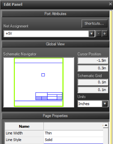
To add a port to the schematic page currently under edit, select the port type you require from the Insert>Add Port menu. Port types available from this menu include:
Analog Ground (AGND)
Digital Ground (DGND)
Voltage
Global Net
Off-Page Port
Select the type of port you require, and the port is assigned to the cursor for placement in the schematic. Place the port as many times as you require, then press the ESC key to unbind the port.
The Display Tab on the Edit panel can be used to set the specific voltage value or net name for the port to be placed.
Adding wires
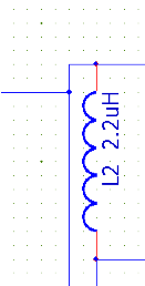 To add a wire between pins on a schematic sheet, simply left-click on the first pin, then mouse over to the next pin and left-click the second pin. PCB123 will interactively draw a wire net that follows your mouse cursor. If you find that you prefer to route the net on a specific path, you can left-click on the schematic sheet to specify an interim location for the net. This function works much like digitizing a layout trace.
Wires can also be initiated and terminated anywhere along an existing wire. Doing so creates a connection to that wire, represented by a connector dot at that location (as shown at right).
Wires can be assigned properties. Wire properties can be accessed by placing the mouse cursor on the wire, then right-clicking to access the context menu, and selecting Properties…
Adding nomenclature

In the schematic, nomenclature is any text, unattached from a part, port or net, that has been added to the schematic for documentation purposes. You are free to use Text, Poly lines, Arcs, Circles and Polygons to add nomenclature to annotate your schematic. You can add these objects to your schematic by selecting Insert from the menu bar. You may also use the Sch Objects toolbar to access these tools. This toolbar is located across the top of your screen and is shown here.
Adding Text – select the function Insert > Add Text. You will be presented with a dialog box into which you can type the text you require. Clicking OK attaches that text box to the mouse cursor and allows you to place the text where needed on your schematic sheet. Press the ESC key to exit text placement mode. Right click the text to access display properties to change such features as font, text size, color, etc.
Properties
For all objects that support properties, properties can be accessed by placing the mouse cursor on the object, then right-clicking to access the context menu, and selecting Properties…
A full discussion of properties can be found elsewhere in this manual. Please refer to “Properties”, page 43.
Cut/copy/paste
The Edit-Cut command deletes the currently selected set of objects and places them into the paste buffer. There is only one paste buffer so only the last cut operation is available for paste.
The Edit-Copy command copies the currently selected set of objects into the paste buffer. There is only one paste buffer so only the last copy operation is available for paste.
The Edit-Paste command makes a copy of the objects in the paste buffer and inserts them into the currently active design.
First, any components in the paste buffer are added to the design by assigning them a new reference designator that does not conflict with one already in the design. Their alpha-prefix is retained.
Next, any complete routes or connections that start and end at pins that are also in the paste buffer will be added to the design. They will retail their original net name with a unique numerical suffix.
Lastly, all text and non-net-attributed polygons will be copied without change. Net-attributed polygons will either inherit a cloned net name or retain their original net names depending on whether their original net names were cloned during the paste operation.
After all objects are created, they will be in a selected state attached to the cursor ready to be placed.
Moving parts
Depending on your experience, there may be a tendency to point at a component, hold down the LMB and drag that component. Though this is allowed, a much easier way is to point at the component and LMB click and release. This attaches the component to your cursor and allows you to do such things as use the RMB for context commands. You click once to select it and begin moving and click again to release it where you want.
Selected parts can be rotated by pressing the r key or mirrored by pressing h (horizontal mirror) or v (vertical mirror).
